This section covers the fundamental elements of symbols used in schematics in Altium Designer. It provides guidelines on style, including line styles, thicknesses, symbol dimensions, scaling rules, and more. Additionally, it outlines graphical representation and layout specific to each symbol type, methods for pin organization, and detailed information about pin functions and symbolic representations to convey electrical characteristics effectively. The section also provides guidance for adding reference designators and symbol names, as well as recommendations for naming pins and managing pin designators, also known as pin numbers.
Note that it is important to check the part ordering information, including notes in the pinout tables to determine if certain pin functions are enabled or disabled for a particular part number. In some cases where symbol pinouts contain a variant set of functionality based on orderable part number, it is important that this variance is understood so the correct pin information is applied to the symbol. This may not be clear just by using the datasheet's pin table.
Style
This convention regulates the presentation of schematic symbols to provide a consistent style across all libraries.
The image below shows a generic representation of a schematic symbol to define standard dimensions.
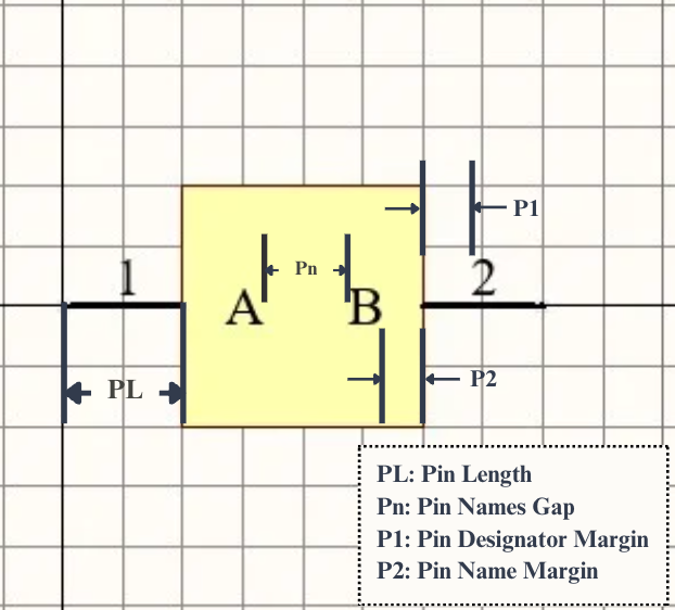
| Property | Standard |
|---|---|
| Pin Color | Black, Hex (#000000), RGB (0, 0, 0) |
| Pin Name Font | Times New Roman |
| Pin Name Size | 10 pixels font size |
| Pin Designator Font | Times New Roman |
| Pin Designator Size | 10 pixels font size |
| Pin Length (PL) | Pin Length - 100 mil for most two-pin components such as Caps/Resistors/Fuses/Inductors/LEDs, etc. Pin Length - 200 mil for most multi-pin components. Pin Length - 300 mil for symbols containing alphanumeric pin designators of 3 or more characters. |
| Pin Name Margin (P2) | 50 mil |
| Pin Designator Margin (P1) | 80 mil |
| Pin Position | Pins should be placed on a 100 mil grid. |
| Pin Visibility | Pin Visibility on if available. |
| Pin Names Gap (Pn) | Opposite Pin names shall not overlap each other. Keep at least a 200 mil (two default grid units) space or gap between opposing Pin Names. |
| Minimum Pin Gap (vertical) | 100 mil (one default grid unit). |
| Symbol Color | Light Yellow, Hex (#FFFFB0), RGB (255, 255, 176) |
| Symbol Border Color | Maroon, Hex (#800000), RGB (128, 0, 0) |
| Symbol Border Size | 1 pixel |
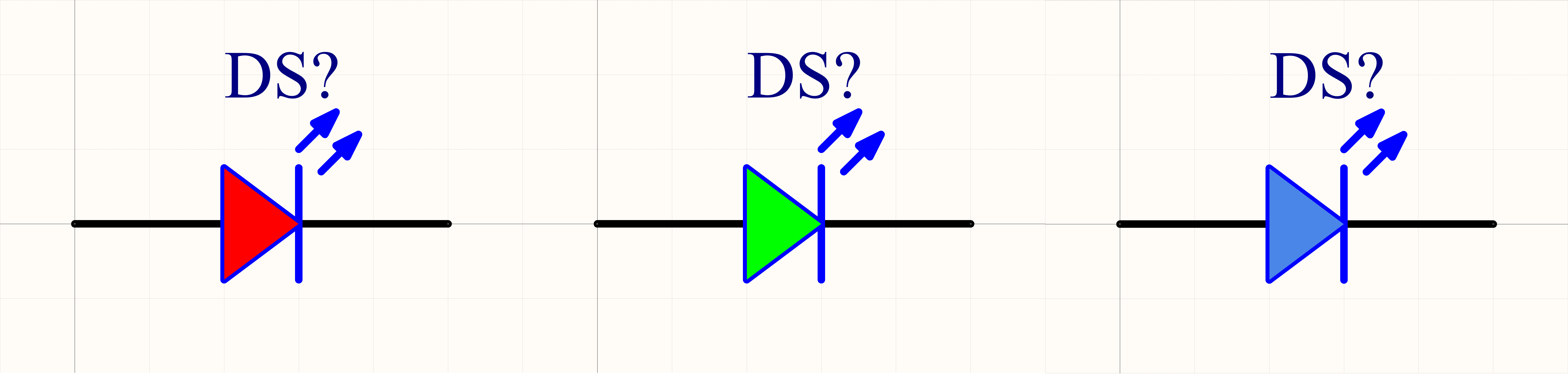
Note: It can be helpful to use a symbol background color for similar component types, for example, power management symbols could have one color background, audio symbols another color, microcontrollers and processors another color, etc. A good example of using a background color for a schematic symbol is LED color. The following examples show LED colors based on the color palette in the 3D Models section of this guide.
Graphical Representation
Symbol Type
The IEEE/ANSI 315-1975 standard, reaffirmed in 1993, is classified as Inactive-Reserved, indicating it has not undergone revision within the last decade and was officially inactivated in 2019. Similarly, IEEE/ANSI 315A-1986 shares the same status.
In response to these developments, the IPC-2612-1 "Sectional Requirements for Electronic Diagramming Symbol Generation Methodology," published in 2010, emerges as a prospective replacement. This IPC standard outlines methodologies for creating new schematic symbols that adhere to industry norms.
While the International Electrotechnical Commission (IEC) 60617 remains a robust resource widely relied upon by engineers globally for its comprehensive array of schematic symbols, our guideline suggests following IPC standards. Below are the Graphic Symbols for Fundamental Items based on the IPC-2612-1 industry standard. The list below is not exhaustive; please refer to IPC-2612-1 for comprehensive details.
| Component Name | Schematic Symbol (IPC) |
|---|---|
| Fixed Resistor | 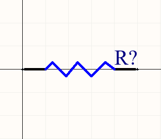 |
| Potentiometer | 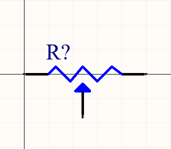 |
| Rheostat | 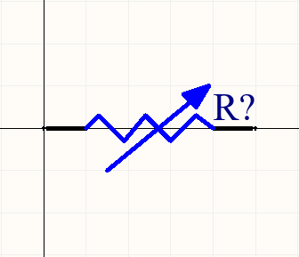 |
| Thermistor | 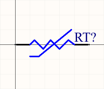 |
| Photoconductive Transducer | 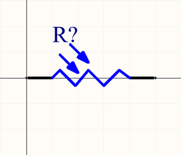 |
| Non-Polarized Capacitor | 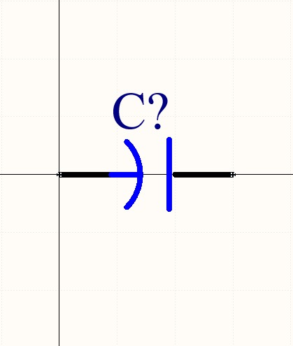 |
| Polarized Capacitor |  |
| Adjustable or Variable Capacitor |  |
| Antenna | 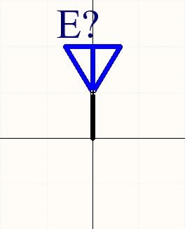 |
| One-Cell Battery | 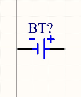 |
| Multi-Cell Battery | 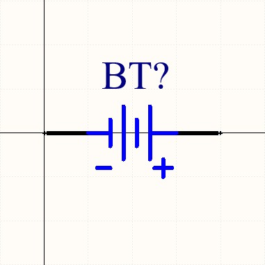 |
| Piezoelectric Crystal | 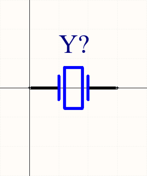 |
| Jack, Phone, 2-Conductor | 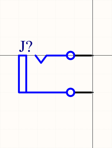 |
| Jack, Phone, 2-Conductor, Interrupting | 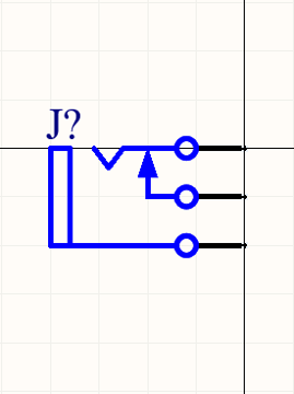 |
| Air-Core Inductor | 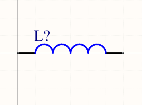 |
| Iron Core Inductor | 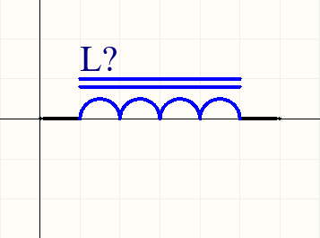 |
| Tapped Inductor |  |
| Adjustable Inductor | 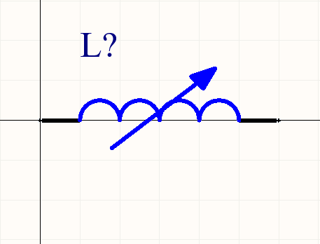 |
| Light-Emitting Diode (LED) |  |
| NPN Transistor | 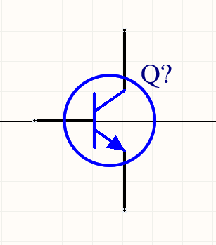 |
| PNP Transistor |  |
| Diode, General | 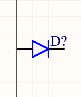 |
| Fuse | 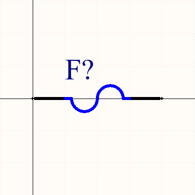 |
| Microphone | 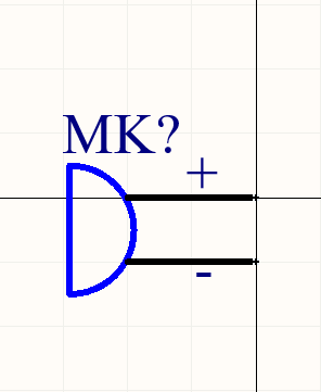 |
| Speaker |  |
Symbol Origin
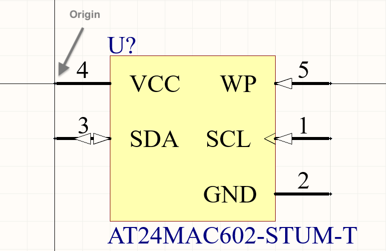
For both symmetrical and non-symmetrical symbols, the symbol origin must be centered at the beginning of the upper leftmost pin.
Grid Settings
The single layout grid established for all the symbols is 100 mil by default. Schematic pins on symbols should be on a 100 mil grid.
Size
The length and height define a boundary area within which the symbol graphic must fit. The symbol can reach the maximum specified dimensions but cannot exceed the defined length and height constraints.
The number of pins affects the length and/or height of components like relays, optocouplers, connectors, etc. Make sure to leave 1 grid or 100 mil space between the top/bottom symbol line and the drawings in the symbols.
| Symbol | Length (mil) | Height (mil) | Symbol Graphic |
|---|---|---|---|
| Fixed Resistor | 500 | 200 | |
| Potentiometer | 500 | 300 | |
| Rheostat | 500 | 300 | |
| Thermistor | 500 | 300 | |
| Photoconductive Transducer | 400 | 400 | |
| Non-Polarized Capacitor | 300 | 200 | |
| Polarized Capacitor | 300 | 200 | |
| Adjustable or Variable Capacitor | 300 | 300 | |
| Antenna | 200 | 300 | |
| One-Cell Battery | 300 | 200 | |
| Multi-Cell Battery | 400 | 200 | |
| Piezoelectric Crystal | 300 | 200 | |
| Jack, Phone, 2-Conductor | 400 | 200 | |
| Jack, Phone, 2-Conductor, Interrupting | 500 | 300 | |
| Air-Core Inductor | 600 | 100 | |
| Iron Core Inductor | 600 | 200 | |
| Tapped Inductor | 600 | 300 | |
| Adjustable Inductor | 600 | 300 | |
| Light-Emitting Diode (LED) | 500 | 400 | |
| NPN Transistor | 400 | 600 | |
| PNP Transistor | 400 | 600 | |
| Diode, General | 300 | 200 | |
| Fuse | 400 | 200 | |
| Microphone | 400 | 300 | |
| Speaker | 500 | 600 | |
Pin Organization
-
All physical pins on the device, including No-Connects (NC), must be represented on the symbol.
-
Multiple pins with identical names are acceptable if specified in the datasheet (GND, OUT, COLLECTOR, etc.).
-
A pin on the symbol may connect to two separate pads. In these cases, represent this connection with a single pin symbol that associates with both pads.
-
-
Prioritize the datasheet's pin table for grouping and positioning pins.
-
Use the "Typical Application" diagram for reference only.
-
Refer to the pin diagram for clarification when necessary.
-
Follow the pin organization standard based on the symbol shape classification in the following section (rectangles, distinctives and connectors).
-
For small pin-count parts, if the datasheet provides a sample symbol, typically found on the first or second page or in the 'Typical Application' section, use this pin organization for the symbol creation.
-
Alignment pins utilizing non-plated holes are not represented as pins on the symbol.
-
All mounting points that require a dedicated copper pad on the PCB, even those without an electrical connection, require representation as a pin on the symbol.
-
For chassis ground pads, NEVER group them together. Each pad gets its own unique pin. If it is connected to GND, then the pin name should be GND. Do not use the old rule of grouping and calling the pin GND_C.
Rectangle-shaped Symbols
-
For IC symbols, generally, inputs are placed on the left side of the symbol and outputs on the right. Distinctive-shaped symbols are exceptions.
-
Position power pins at the upper left-hand side of the symbol. Power pins should be the first pins at the top left of the symbol. Order power pins following the same organizational order as the datasheet.
-
Position ground pins at the lower right-hand side of the symbol. The ground pins should be the last pins at the bottom right of the symbol. Order power pins following the same organizational order as the datasheet.
-
For symbols exceeding ten (10) pins, a minimum spacing of 2 pin positions should be maintained between power pins and other signal pins.
-
Where feasible for single-part symbols, strive for a balanced pin distribution to avoid excessive concentration on one side.
-
When the pin count is greater than or equal to 80, use multi-part symbols following these guidelines:
-
Ensure no more than 45 pins are on one side of a sub-symbol to avoid overcrowding and maintain readability.
-
Break up sub-symbols by major functions to enhance organization and ease of understanding (GPIOs, operating mode, system control, USB function module pins, etc..)
-
Create separate symbols specifically for power and ground connections to streamline the design.
-
Group pins based on their function as detailed in the pin function/configuration section of the datasheet.
-
For large pin count parts, each sub-symbol should have at least 10 pins.
-
Name each sub-symbol with the reference designator followed by a letter (??A, ??B, ??C, etc.).
-
-
Consider utilizing multi-part symbols for standard components with multiple isolated instances (resistor networks, quad op-amps, multiple voltage regulators, etc.).
-
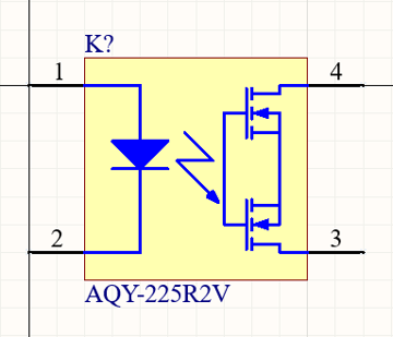
For components where pin connections alone may not clearly convey their function (level shifters, optocouplers, isolators, and similar devices), consider incorporating a simplified internal functional representation within the symbol.
-
Prioritize grouping pins based on their function, not their pin number.
-
Pins within the same functional pin group should be placed above or below each other, with zero grid spaces between them.
-
If the datasheet suggests connecting a pin to VSS, VCC, or ground, ensure that the pin is grouped with the corresponding pin(s) as indicated in the datasheet.
-
Introduce one or two grid spaces between distinct functional pin groups.
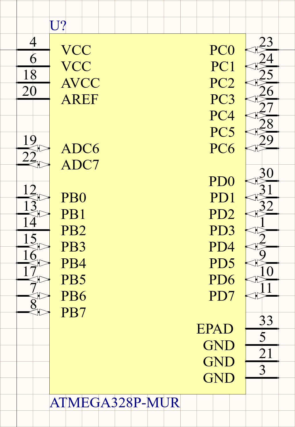
The example below demonstrates how pins with similar functions are grouped. For instance, signals PB0 through PB7 might be grouped together, followed by PC0 to PC6, and lastly, PD0 to PD7, all grouped by their respective functionalities.
Below is a second example to demonstrate proper organization, with inputs and I/O on the left and outputs and I/O on the right.
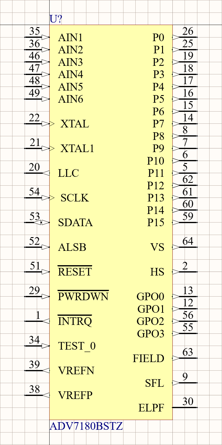
-
-
It is suggested that the differential signal pairs pins be grouped together. In the example below, there are pin groups (DP0n, DP1n, etc., and DP0p, DP1p, etc.) where the first group is the differential negative input signal, and the second group is the differential positive input signal. In such cases, the signals should be grouped as DP0p with DP0n, DP1p with DP1n, and so forth.
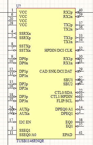
-
Maintain data bus signals together on the same side of the symbol.
-
For symbols containing standard interfaces (e.g., JTAG, SPI, I2C), group the corresponding pins following the established order as defined in Table 7. Standard Interfaces should have priority over general purpose I/O and be placed on the symbol above general purpose I/O.
| JTAG | I2S | I2C | SPI | SMBus | PMBus |
|---|---|---|---|---|---|
| TDI | Master Clock (CLK, MCLK) | Clocks (SCL) | Clocks (SCLK, CLK) | Clocks (SMBCLK) | I2C Clock (SCL) |
| TDO | Serial Clock (SCLK, BCLK, I2SCLK) | I2C Data (SDA) | In (SDI, DI, DIN, SI, MOSI) | Data (SMBDAT) | I2C Data (SDA) |
| TCK | Word Clock (WCLK, LRCLK) | Addresses (ADn) | Out ( SDO, DO, DOUT, SO, MISO) |
Alert (SMBAlert#) | Alert (SMBAlter#) |
| TMS | In (DIN) | Select (SS, CS, nCS, CN_N, nSS, STE) | Control (CONTROL) | ||
| TRST | Out (DOUT) | Write Protect (WP) | |||
| Selects (WS) | Addresses (ADn) |
| Ethernet MII | Ethernet RMII | RS232 | RS442 / 485 | USB |
|---|---|---|---|---|
| Management Clock (MDC) | Reference Clock (REF_CLK) | Data Terminal Ready (DTR) | TXDA, TxD- | VBUS |
| Management IO (MDIO) | Transmit Enable (TX_EN) | Data Set Ready (DSR) | TXDB, TxD+ | D- |
| Others are same as RMII | Transmits (TX0, TX1) | Data Carrier Detect (DCD) | RXDA, RxD- | D+ |
| Receive Error (RX_ER) | Ring Indicator (RI) | RXDB, RxD+ | IN | |
| VFReceives (RX0, RX1) | Clear to Send (CTS) | Reference (SC, REF) | ID | |
| Request to Send (RTS) | GND | |||
| Transmit (TXD) | ||||
| Receive (RXD) |
Distinctive-shaped Symbols
Operational Amplifiers (Op-amps)
-
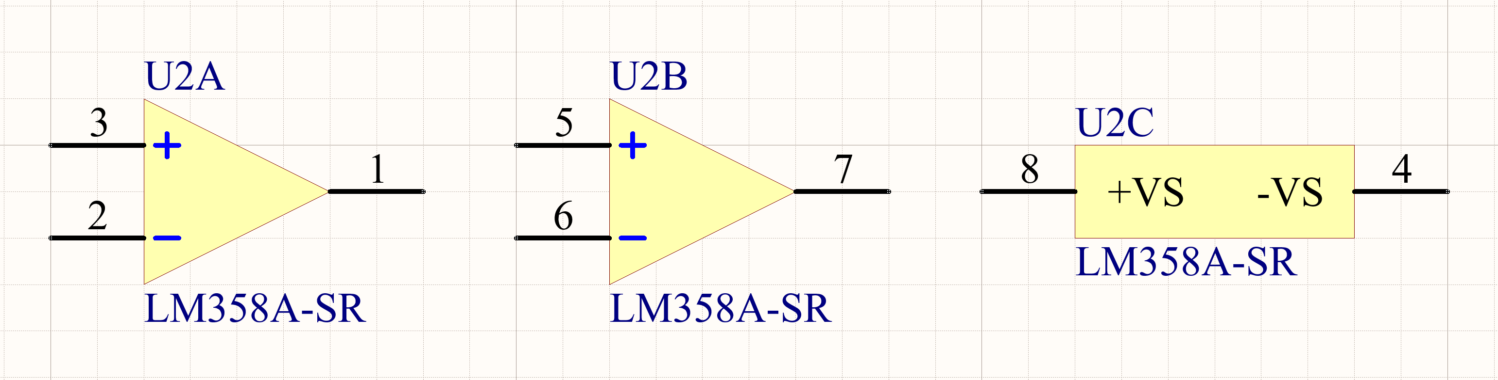
Distinctive-shaped symbols of op-amps are drawn as an isosceles triangle.
-
Differential input and output pin names are hidden.
-
Align pins on each side of the symbol to end on a grid line.
-
Create a separate symbol part for power pins and other functional pins that are not differential input/output pins, including "Not Connected pins" (NC).
-
Pin types for op-amps should be categorized as high-impedance for differential inputs and passive for outputs.
Op-amp example:
Logic Gates and Buffers
-
Logic pin names should be hidden.
-
Logic power pin names, if included in a logic symbol, should also be hidden.
-
Logic power pin names (VCC, BDD, BEE, GND, etc.) that are included in a separate power/control symbol part should be visible.
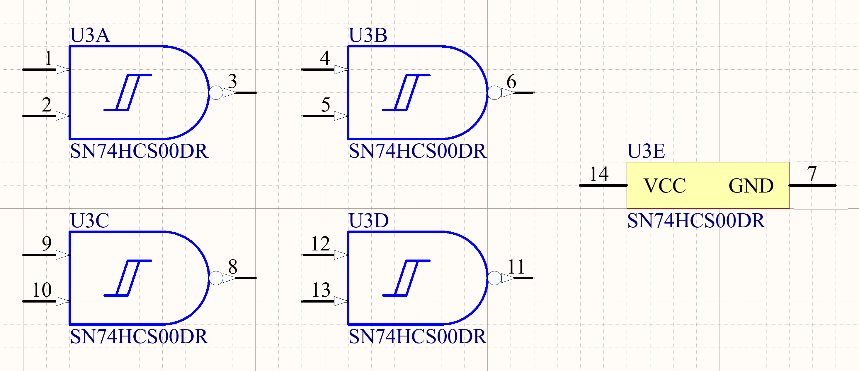
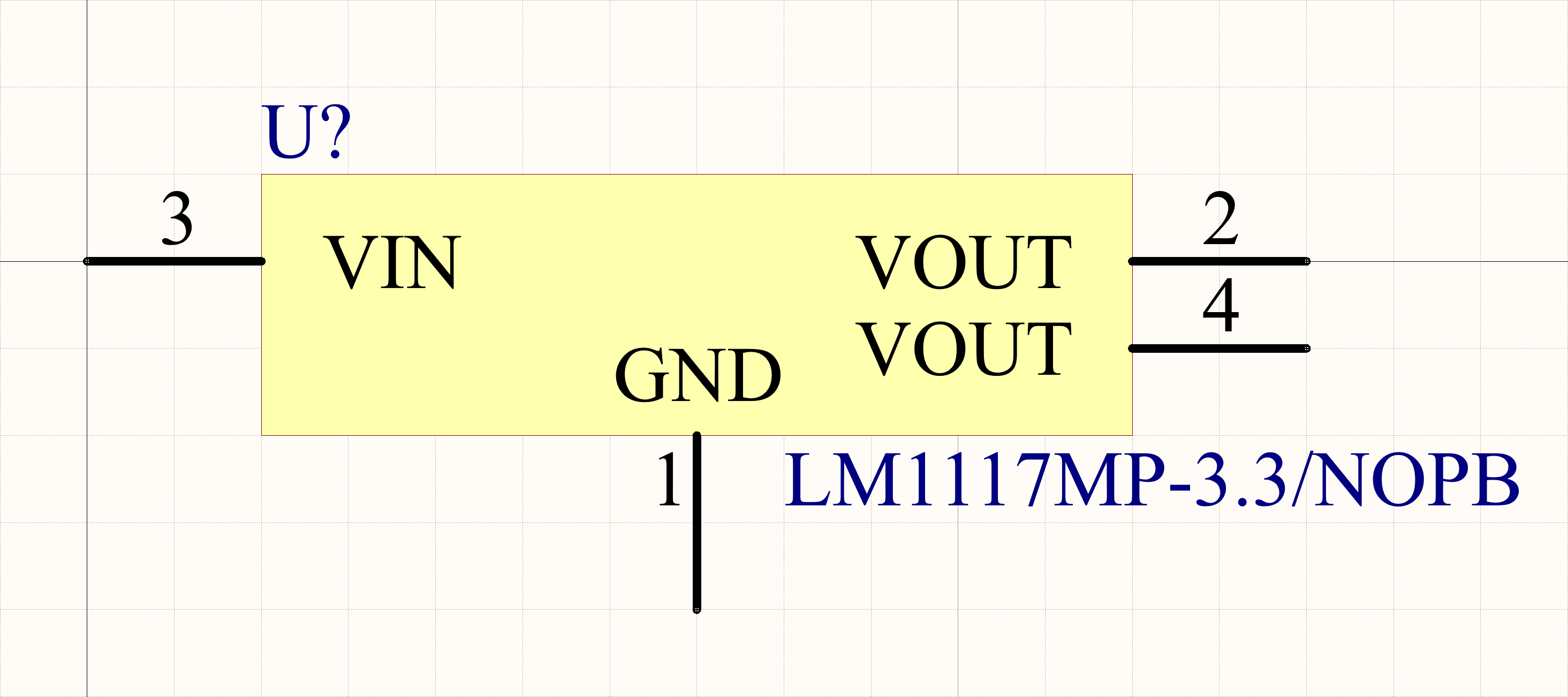
Voltage Regulators
-
A voltage regulator is a rectangle with ground pins on the bottom, input on the left side, and output on the right.
-
For the vertical GND/ADJ pin, set the pin designator and the pin name to be horizontal.
-
If there are multiple input, output, ground, or adjustment pins, they should be drawn side by side.
-
The "Electrical Type" of input and output is "Power".
-
It is recommended that the component name (part number) be positioned to the right of the vertical pin at the bottom of the symbol, so as to not overlap it in the case of long part numbers.
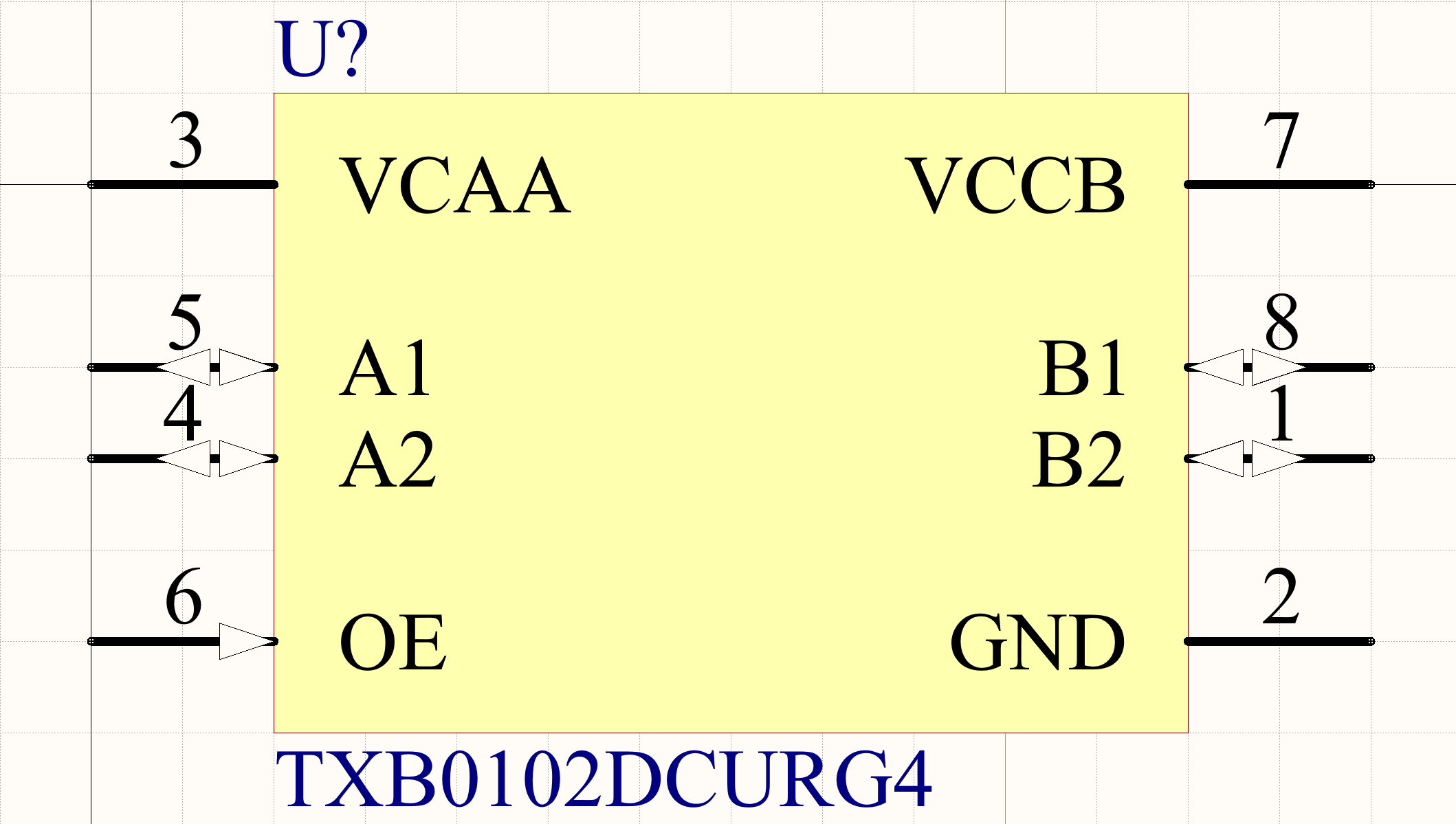
Level Shifters
For parts like level shifters, it makes sense to break the VDD rules and split the symbol into input on the left and output on the right, including any output power supply voltage.
Connectors
-
For single-row connectors, the pins must be all on the right side.
-
For a double-row connector, the pins must be on both the right and the left sides.
-
For multi-row connectors (more than two rows), create a symbol part per connector row.
-
No extra spaces between pins.
-
For single-row connectors with more than 50 pins, split the symbol equally into multiple parts.
-
For some connectors (RJ45, USB, DSUB, Coaxial, etc.), the symbol can represent the geometry of the connector.
-
Indicate male/female terminals in connectors where required.
-
Connector symbol representation per IPC-2612-1.
-
The numbering style should also be set per the datasheet/land pattern suggestion. If not in the datasheet, follow the sequence 1,2,3, etc., based on the datasheet footprint orientation in sweeping order from left to right and top to bottom.
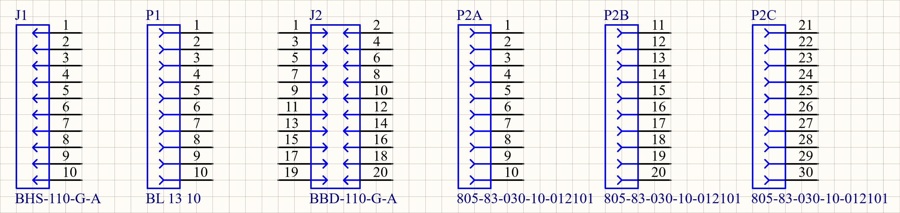
J? or P? The IPC-2612-1 suggests that any connector or assembly the connector is on that is fixed in place, does not move and is not removable, be designated as J (i.e., a motherboard connector, a panel mounted connector, etc.). Any connector or assembly the connector is on that is movable or removable, be designated as P (i.e., daughter board connector, cable or wire harness connector, etc.).
Reference Designator
The reference designator should be placed on the left side of the symbol graphics and above the symbol graphics. If there is a vertical pin at the top of the symbol, place the reference designator above the symbol graphics and to the right of the vertical pin (or the last pin in the case of multiple vertical pins). This will ensure that long reference designators do not overlap the vertical pin.
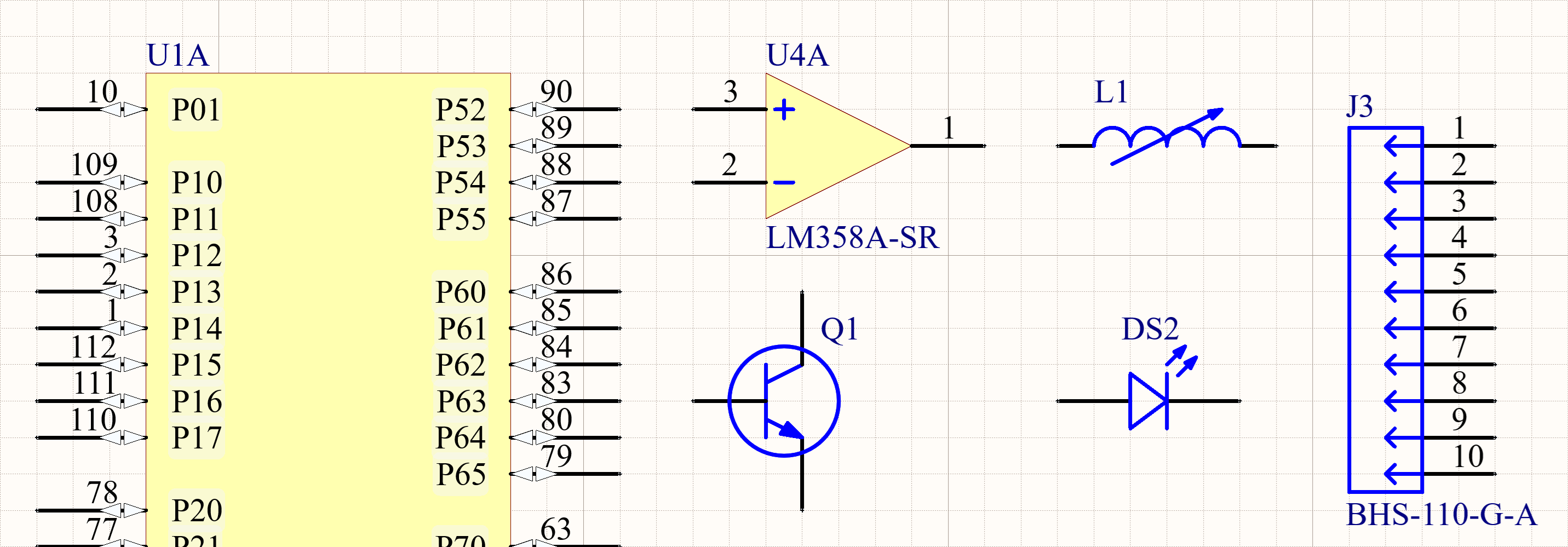
The table below lists commonly used designators and may not necessarily comply with all standards. The commonly used reference designator list is preferred.
For ANSI Y32.2/IEEE Std. 315 and IPC-2612-1, the below list is not exhaustive; please refer to the standard list of class designation letters in ANSI Y32.2/IEEE Std. 315, Section 22.4 or index A.
| Terminology | IEC | ANSI Y32.2-1975 and IEEE Std 315-1975 |
IPC-2612-1 | Commonly Used |
|---|---|---|---|---|
| Amplifier | A | AR | AR | AMP |
| Attenuator/Isolator | AT | AT | ||
| Antenna | AE | E | ANT | |
| Battery | G | BT | BT | BT,BAT |
| Capacitor | C | C | C | C |
| Circuit breaker | Q | CB | CB | CB |
| Contactor | K | K | K | K |
| Converter | U | A,U,MG | U | |
| Crystal filter | Z | FL | FL | FL |
| Crystal transducer | B | Y | Y | Y,XTAL |
| Connector, Plug (movable portion) | P | P | P | |
| Connector, Jack (stationary portion) | J | J | J | |
| Transformer | T | T | T | T |
| Diode | V | D | D, CR | D |
| Infrared Diode | IR | |||
| Display Device | DS | DS | DS | |
| Filter | Z | FL | FL | FL |
| Fuse | F | F | F | F |
| Ferrite Bead Ring | E | FB | ||
| Inductor | L | L | L | L |
| Integrated Circuit | IC | U | U | U |
| Jumper wire | W | W | W | W |
| Light-Emitting Diode (LED) | DS | DS | ||
| Loudspeaker | B | LS | LS | LS |
| Microphone | B | MK | MK | MIC |
| Modulator | U | A | U | |
| Motor | M | B | B | M |
| Mechanical part | MP | MP | ||
| Oscillator | G | Y,G | G | Y,OSC |
| Potentiometer | R | R | POT | |
| Pushbutton | S | S | PB,S,SW | |
| Relay | K | K | K | K |
| Resistor Shunt (resistor) |
R | R | R | R |
| Selector Selector Switch |
S | S | S,SW | |
| Supply Supply device |
G | A, PS | PS | |
| Terminal | X | E | E | E |
| Thermistor | R | RT | RT | RT |
| Thyristor Transistor |
V | Q | Q | Q |
| Test point | TP | TP | TP |
Name
The value of the component name (also known as value) corresponds to the component’s manufacturer orderable part number for all components. The name (value or orderable part number) object should be placed at the left and below the symbol graphics.
Electrical Characteristics
Pin Types
While symbols themselves don’t have electrical characteristics, the components they represent do and these may vary depending on your specific electronic design automation tool. Here are some of the key pin types categorized by their electrical characteristics:
-
Passive: Used for pins that do not actively drive a signal (resistor pins, capacitor pins, NC pins, IC configuration pins, and the anode/cathode of a diode).
-
Input: Used for pins that receive a signal (enable pins, reset pins, memory address pins, and input clocks, etc.).
-
Output: Used for pins that drive a signal to another component (state flag pins and any signal named "output").
-
Input/Output (I/O): Used for pins that can both receive and drive a signal, depending on the circuit configuration (general purpose I/O pins).
-
Analog: Used for processing analog signals (analog input pins on a sensor or microcontroller).
-
Ground: Used for pins that provide the return path for current and/or are common reference voltage.
-
Open-Collector/Open-Drain/Open-Emitter: These pin types should be used only when the component’s datasheet explicitly specifies an open-collector (i.e. for BJTs), open-drain (i.e. for FETs), or open-emitter (i.e. for BJTs or FETs), indicating the respective collector, drain, emitter, or source pin operates in this configuration.
-
High-Impedance: Used for pins that are in a high-impedance state, meaning they draw minimal current and have minimal impact on the circuit (gate pin of a MOSFET).
-
Power: There is a separate category for power pins that includes both positive/negative rails and GND (Ground).
Pin Description
If available, this pin property can be used to describe the pin function(s).
Pin Names
-
When naming pins, prioritize the pin table provided in the datasheet. If necessary, refer to the pin diagram for additional guidance.
-
If a datasheet includes a pin table and a diagram but only the table lists pin numbers and names, use the table. This is common in transistor datasheets, where diagrams may label pins without numbers. Refer to the table for accurate mapping.
-
Some parts have adjustable and fixed voltage versions, indicated by the part number suffix (e.g., LM1117MP-1.8 for fixed 1.8 V). Pins labeled ADJ/GND should be called GND for fixed versions and ADJ for adjustable versions.
-
Maintain the original order of the pin name as it appears in the pin table.
-
Pin names must match the datasheet exactly, including capitalization, without abbreviations or expansions, as instructed in IPC-2612-1. The exceptions are in the table below to standardize some of the most common pin names.
Table 9. Common Pin Name Standardization Datasheet Pin Names Standardized Pin Names Ground, GROUND, GND, ground GND Analog Ground, Analog GND, AGND, GNDA AGND Digital Ground, Digital GND, DGND, GNDD DGND Power Ground, Power GND, PGround, PGND, GNDP PGND Thermal Pad, Exposed Pad, EPAD, TP, TPAD, THPAD, ground pad EPAD Not Connect, NC, No Connection, Do Not Connect NC Reserved, Rsvd, RESERVED, RSVD RSVD Vcc, VCC, vcc VCC Vdd, VDD, vdd VDD Vss, VSS, vss VSS -
Name the pins as specified in the datasheet. If not specified in the datasheet:
-
Use + and - for all types of electrolytic capacitors.
-
Use K and A for diodes.
-
Use E, B and C for BJT transistors.
-
Use D, G and S for MOSFET transistors.
-
-
If a datasheet does not specify a pin name and the pin is unconnected or unused, name it "NC" (No Connect).
-
For an LED part that has multiple colors, if the datasheet contains no pin naming, name the pins RK (for red cathode), GK (for green cathode), BK (for blue cathode), RA (for red anode), GA (for green anode), and BA (for blue anode).
-
For multi-device components with polarity, such as a dual transistor or dual diode, if the datasheet contains no pin naming, name the pins according to Table 10.
Table 10. Suggested Pin Names for Multi-Device Components with Polarity Transistor Diodes MOSFETs RGB LEDs E1, E2, etc. K1, K2, etc. D1, D2, etc. RK1, RA1, RK2, RA2, etc. B1, B2, etc. A1, A2, etc. G1, G2, etc. GK1, GA1, GK2, GA2, etc. C1, C2, etc. S1, S2, etc. BK1, BA1, BK2, BA2, etc. -
If the component is a BIDIRECTIONAL ESD suppressor and there are no pin names in the datasheet, name the pins 1 and 2. In the following image, pin 1 is on the left and pin 2 is on the right.
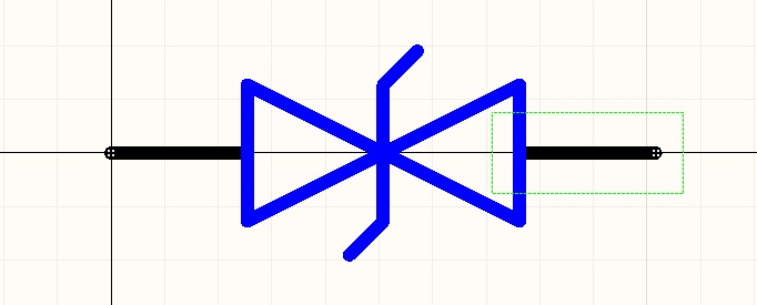
-
If the datasheet does not contain names and the part does not match any of the other rules, name the pins numerically, starting with 1 and increasing.
-
Special case for network resistors and capacitors.
-
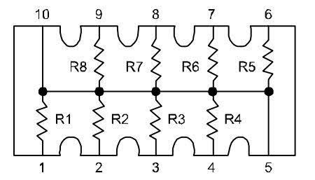
If the datasheet does not provide pin names, name the pins 1,2,3 starting from the bottom left corner and going to the right and around for a horizontal footprint or top left corner and going down for a vertical footprint.
-
For the example below: Pin 1 = 1, Pin 2 = 2, … Pin 7 = 7, Pin 8 = 8. For this particular example, you can build this symbol as a singular part symbol or a multipart symbol depending on your specific case.
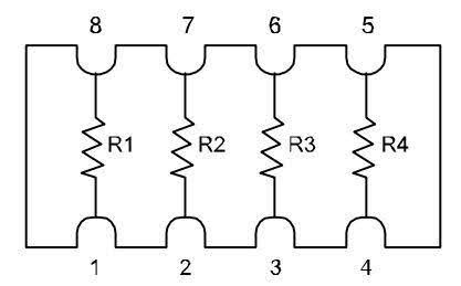
For the example below: Pin 1 = 1, Pin 2 = 2, … Pin 9 = 9, Pin 10 = 10.
-
-
Pins used for shielding purposes are named "SH".
-
If there are no pin names in the datasheet, the following pin names should be used.
Table 11. Recommended Pin Names Type Abbreviation Description Plated Through-hole PTH Hole with copper Non-plated Through-hole NPTH Hole without copper Mounting Hole MTG Hole with or without copper for mounting purposes Test Point TP Holes or pads used for testing purposes -
For 2-terminal passive components such as resistors, capacitors, diodes, inductors, etc., hide the Pin Name.
-
For the tab pin of a DPAK or SOT component: if the datasheet does not name the tab and does not identify that it needs to be connected to anything, name it MNTPAD.
Pin Designator
For 2-terminal passive components such as resistors, capacitors, diodes, inductors, etc., hide the Pin Designator.