The footprints section of this guide provides comprehensive guidelines for creating consistent and accurate footprints in CAD libraries. It includes recommendations for pad designators, also known as pad numbers, detailing the standard practices for assigning pad names. For Surface Mount Technology (SMT), it covers land pattern naming conventions, pad shapes, and thermal pad design. For Through-Hole Technology (THT), it addresses land pattern naming conventions, pad shapes, and hole sizing.
Additional guidelines are provided for footprint origin placement and mechanical layer usage. Specific recommendations are also included for axial components, dual-in-line package (DIP) components, and other footprint-specific details, ensuring precision and ease of use throughout the layout process.
When designing footprints, it is recommended to create all three IPC variations of land pattern geometry, along with any recommended land patterns provided in the datasheet, if available. This ensures that the libraries will be suitable for low-density, moderate-density, and high-density component applications. We recommend creating the recommended land pattern footprint using the units specified in the datasheet.
Pad Designator
-
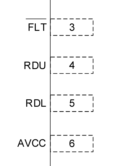
Pads should be designated (numbered) exactly as they are in the datasheet.
-
For thermal pads, exposed pads, and tabs, always assign them the next available pad designator, even if the datasheet designates them as exposed pad, thermal pad, or tab, etc.
-
-
If the datasheet does not include numbers and the part is not a BGA and/or LGA, designate the pads numerically, starting with 1 and increasing. For an 8-pin component with a ground pad, designate the pad as 9.
-
For polarized components, the cathode pad for diodes and LEDs should be designated as Pad 1, and the anode pin should be designated as Pad 2. For polarized capacitors and batteries, the positive pin should be designated as Pad 1, and the negative pin should be designated as Pad 2.
-
When a polarized component has an anode or negative pin polarity mark on its package, designate the cathode or the positive pin as Pad 1 and the anode or negative pin as Pad 2.
-
-
If the datasheet does not include numbers, and the part is a BGA, designate the pads by giving each row a letter starting with A, and each column a number starting with 1. You should end up with a grid where each pad’s number is the combination of the row letter and the column number.
-
If the datasheet identifies pins as terminals or contacts (Terminal 1, Terminal 2, Contact 1, Contact 2, etc.), designate the pads as 1, 2, etc.
-
There are two ways to design parts with multiple pins associated with a single pad. Below is an example of such a part.
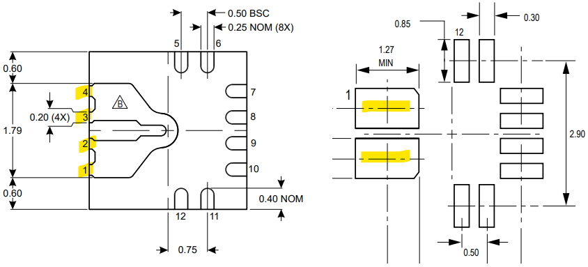
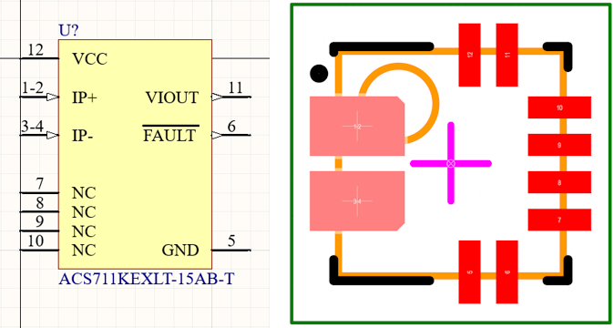
One way to design these parts is to have a single symbol pin designated with a pin number of 1-2, and the footprint has a pad designated as 1-2. For example, the Allegro Microsystems ACS711 device below was designed following this first method.
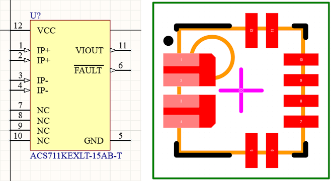
The second way is to have two symbol pins, one designated as 1 and the other designated as 2. Use two separate pads in the footprint designated as 1 and 2 and then cover those pads with a region in the shape of the single pad specified in the datasheet. Whichever approach is used, be aware that Altium Designer may issue warnings. The same example was designed following this second method.
-
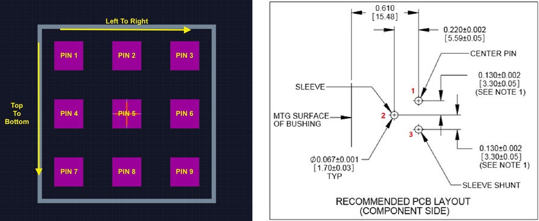
If the datasheet does not include pin numbers, or the datasheet does not number all the pins, designate the pads 1,2,3,... based on the datasheet footprint in sweeping order from left to right and top to bottom. Priority is given to signal pins followed by structural/mounting pins (see example).
As an example, the 5025700893 part number from Molex is a microSD Memory Card Connector. In the datasheet, the Pin Number and Names are described for the pin 1, 2, 3,...8.
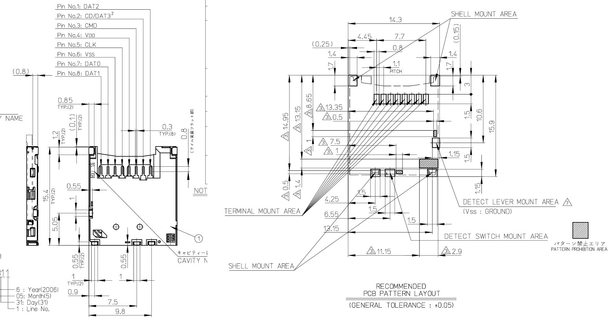
However, the datasheet does not give pin names or numbers to shell mount pins, detect switch mount pins or the detect lever mount pin. Designate the pads for those pins as 9, 10, 11,...,14, as listed below.
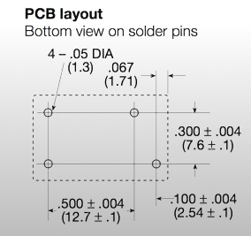
Pad Designator Pin Name 9 Shell Mount 1 (No pin) 10 Shell Mount 2 (No pin) 11 Detect Lever 12 Shell Mount 3 (No pin) 13 Detect Switch 14 Shell Mount 4 (No pin) The following example has a recommended land pattern from the “bottom view,” in this case, flip the footprint from left to right and follow the rule above.
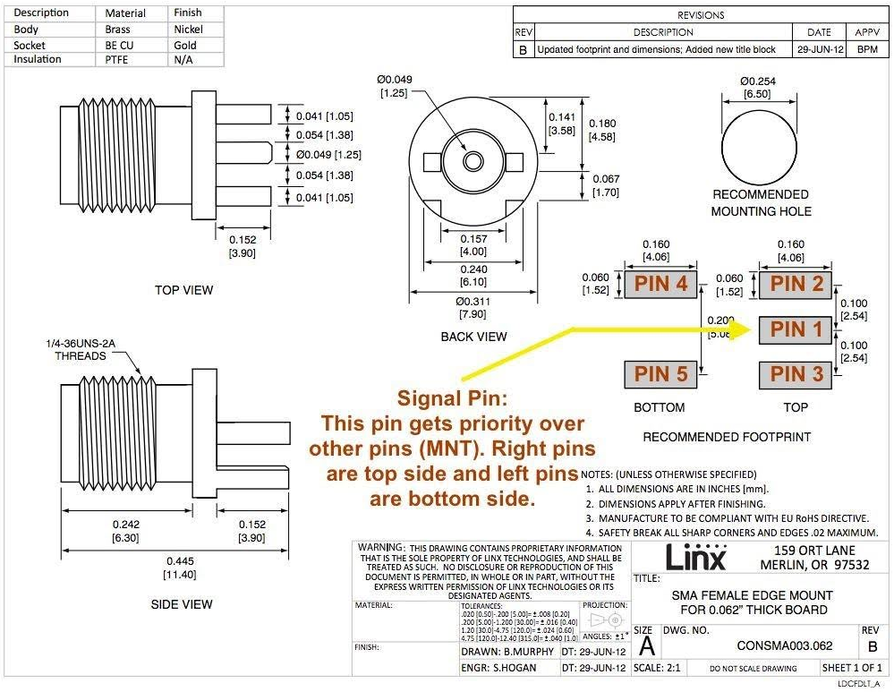
The following example has the recommended land pattern with pads on the top and bottom of the board. Designate the pads on the top side first, followed by the bottom side. Start with the signal pins and then the mounting pins.
-
For headers and receptacles (male and female) that do not have pin numbers defined in the datasheet, designate the pads 1, 2, 3… starting on the bottom left corner and alternate. See examples below.
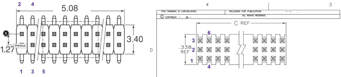
-
Special case for network resistors and capacitors: If the datasheet does not provide pin numbers, designate the pads 1, 2, 3 starting from the bottom left corner and going around for a horizontal footprint or top left corner and going down for a vertical footprint.
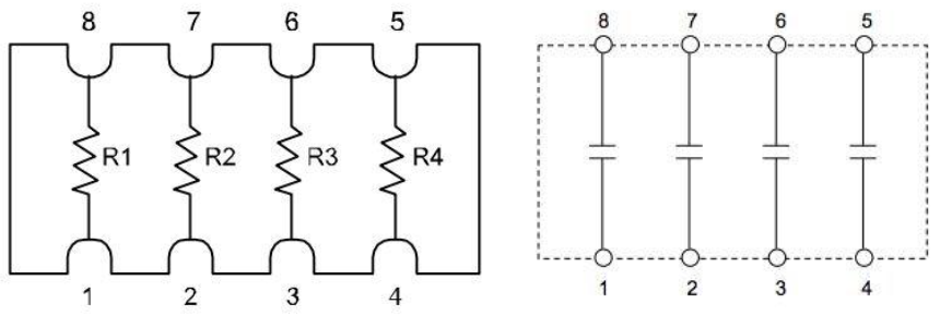
-
When the pin numbers are not shown in the datasheet, for packages such as QFN, SOIC, SO, etc., locate the pin 1 marker (it can be a dot or bevel), then designate the pads while going around as shown in this diagram below.
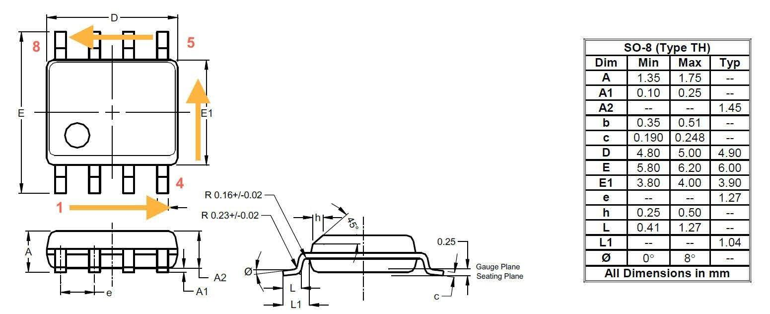
-
When the pin numbers are not shown in the datasheet for DPAK-style packages with a trimmed pin designate the pads as shown below.
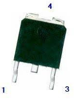
-
If the pin numbers are not available in the datasheet, the tab pad of a DPAK, SOT or TO- component is ALWAYS the next available pad designator number.
Surface Mount Technology (SMT)
Land Pattern Naming Convention
This style guide suggests following IPC-7351B Land Pattern Naming Convention for SMD Packages (Section 3.1.5.5, Table 3-23) and for non-standard SMT land patterns, as well as IPC-7x51 naming convention for connector land patterns, followed by internal manufacturer package code ending with the density level. For example, the internal manufacturer package code for QFP50P1600X1600X170-100_PLQP0100KB-B_N is PLQP0100KB-B.
Thermal Pads
-
Vias:
-
If the datasheet specifies a via in thermal pad requirement, include the vias in the footprint. The datasheet must provide a minimum number of vias. If this information is not present in the datasheet, do not add vias to the footprint.
-
Hole Diameter:
-
If the datasheet specifies a hole diameter, use the specified hole diameter (if the range is specified, use the smallest).
-
If the datasheet does not specify a hole diameter, use a 0.3 mm hole diameter.
-
-
Pad Diameter:
-
If the datasheet specifies a pad diameter, use the specified pad diameter (if the range is specified, use the smallest).
-
If the datasheet does not specify a via hole diameter nor a via pad diameter, use a 0.6 mm via pad diameter and a 0.3 mm via hole diameter.
-
If the datasheet specifies a via hole diameter but not a via pad diameter, then the via pad diameter = 0.3 mm + the via hole diameter.
-
-
Via Spacing:
-
If the datasheet specifies the via spacing, use the specified spacing in the footprint. If a range is specified, use the nominal value.
-
If the datasheet does not specify via spacing, arrange it in an evenly spaced grid. (For example, thermal pad = 5 mm x 5 mm, 9 via requirement. Create a 3x3 via grid with spacing = 5 mm / (3 vias +1) = 1.25 mm spacing).
-
-
-
Paste Mask:
-
For non-IPC-compliant footprints, if the datasheet recommends a footprint and a paste mask (stencil), implement the recommended paste mask/stencil design.
-
For IPC-compliant footprints, the IPC-7351B default paste mask for thermal pads is 40% of the overall land area. The paste mask on the thermal pad is a single square for thermal pads 4.0 mm or less. Greater than that size, the thermal pads are typically segmented into multiple patterns.
-
Pad Shape
IPC-7351B recommends using oblong or rounded land pattern pads over rectangular pads. This style guide recommends that IPC-compliant footprints always use oblong pad shapes, except for thermal pads or tabs.
In general, ICs will have an oblong pad shape and discrete components will have a rounded pad shape.
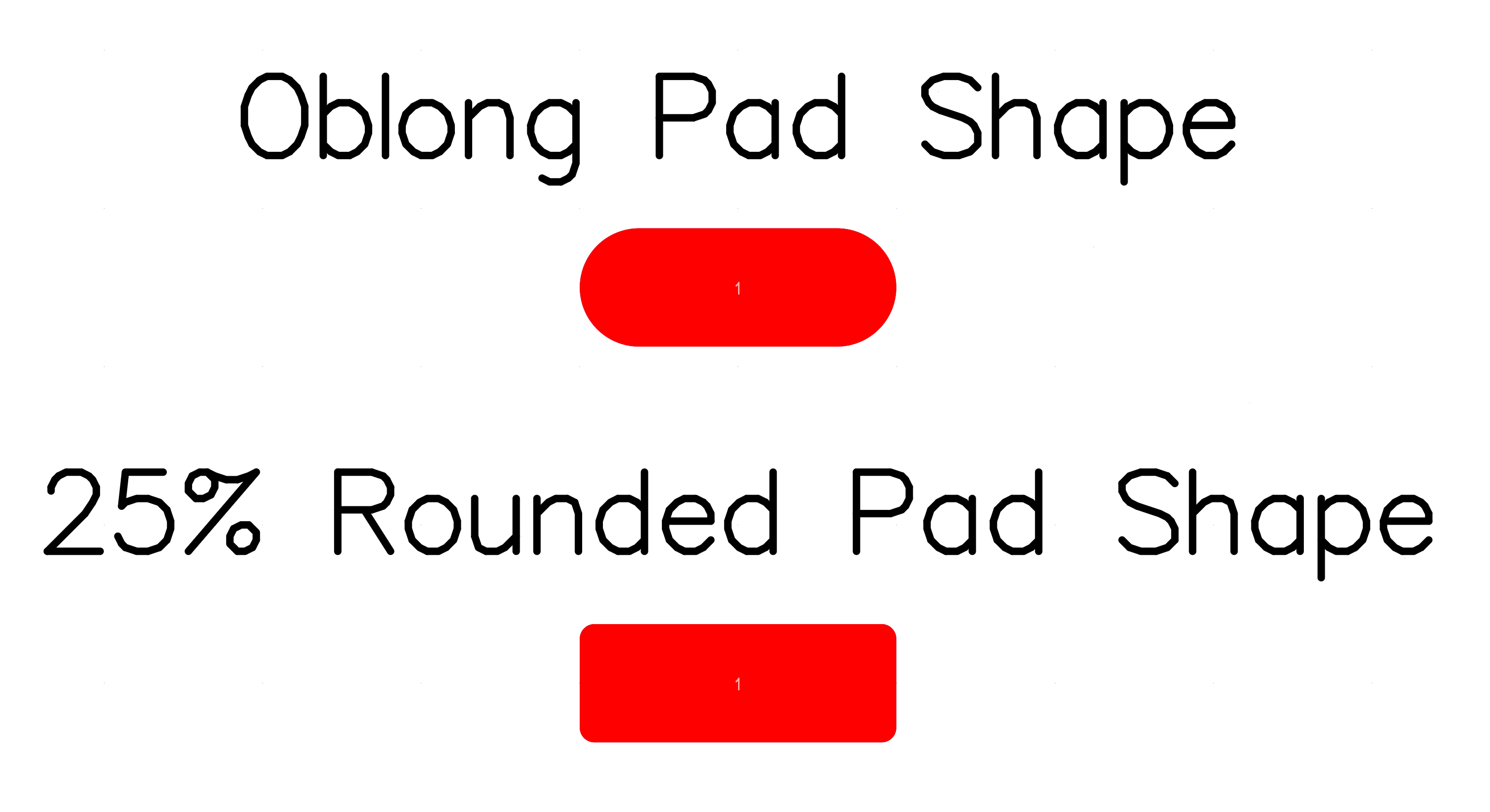
Note: An exception to this recommendation occurs when the heel portion of the land pattern has to be trimmed due to the component body standoff being less than the paste mask stencil thickness or the heel having to be trimmed due to “Thermal Pad” interference. In these two cases, the rectangular pad shape is preferred to compensate for the reduction in copper area of the land pattern pad length.
Note: Some datasheets do not directly identify the copper and paste mask dimensions and instead use SL/SP/SR.
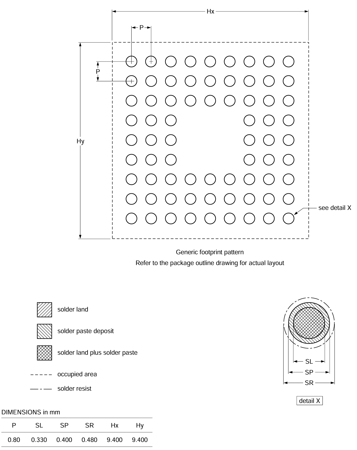
SL = solder land; this is the size for the copper pads.
SP = solder paste deposit; this is the size for the paste mask.
SR = solder resist; this is the size of solder mask opening.
Through-hole Technology (THT)
Land Pattern Naming Convention
This guideline suggests following the IPC-7251 Naming Convention for Through-Hole Land Patterns and Non-standard PTH Land Patterns. It also suggests following the IPC-7x51 Naming Convention for Connector Land Patterns. Then, add the internal manufacturer package code after the IPC name, and end with the density level.
Pad Shape
-
For 2-pin polarized packages: Use a rounded rectangle pad shape for pad 1 and a circular pad shape for pad 2.
-
For 2-pin non-polarized packages: Use circular pad shapes for both pads.
-
For multi-pin through-hole footprints with more than two pins, pin 1 should be rounded rectangle and all other pins circular. For the rounded rectangle pad shape, use a 25% corner radius.
Hole Sizing
Plated Through-Holes
-
If the datasheet specifies a finished hole size and a pad diameter, follow the datasheet recommendation.
-
If the datasheet does not specify a finished hole size nor pad diameter but specifies the maximum lead diameter, use IPC-2222 and IPC-2221 to calculate minimum plated through-hole size and pad diameter. This style guide suggests using the formulas for IPC level B.
-
If the datasheet provides a hole tolerance, follow the datasheet with the exception that for tolerances that are less than ±0.08 mm, for plated through-holes, use ±0.08 mm for the tolerances. If the datasheet does not specify hole tolerances, use ±0.08 mm for plated through-hole.
Non-plated Through-Holes
-
If the datasheet specifies a finished hole size, follow the datasheet recommendation.
-
If the datasheet provides a hole tolerance, follow the datasheet with the exception that for non-plated through-holes with tolerances less than ±0.05 mm, use ±0.05 mm for the tolerance. If the datasheet does not specify hole tolerances, use ±0.05 mm for non-plated through-holes.
-
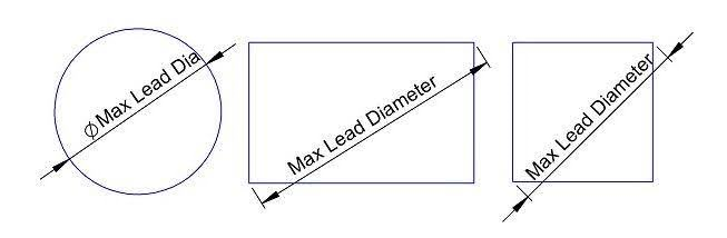
For leads that are not circular, the maximum lead diameter is the hypotenuse, which is the square root of the maximum length square plus the maximum width square.

-
The hole sizes specified are for finished holes. The manufacturer will increase all hole sizes to account for plating.
-
If the datasheet does not mention or show a lead shape (circle/rectangle/square), it is important to determine the actual lead shape.
Plated Through and Non-plated Through Slots
The same specifications for Plated Through-Hole and Non-plated Through-Holes apply to plated-through and non-plated through slots.
Axial Components
To find the pitch (e) for axial components, use the following formulas:
Axial Lead Pitch is: e = D + 2(L + R + b/2)
Minimum Bend Radius is: R = mb
b: Maximum lead diameter.
D: Part length, including weld beads, if any.
L: Lead length extension; lead length extension is equal to 1 lead diameter, but not less than 0.8 mm.
m: Bend radius multiplier, according to Table 12.
R: Minimum bend radius, which is equal to the bend radius multiplier times the maximum lead diameter.
e: Pitch.
| Maximum Lead Diameter (mm) | Bend Radius Multiplier (m) |
| Up to 0.8 mm | 1 diameter |
| From 0.8 mm to 1.2 mm | 1.5 diameters |
| Larger than 1.2 mm | 2 diameters |
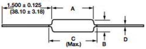
Note: In cases where two body lengths are shown as in the example below, dimension C should be used for the maximum body length:
Dual-In-Line Package (DIP) Components
-
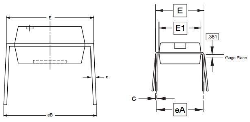
If there is no recommended footprint in the datasheet or MFG website, center-to-center spacing between the two columns of holes = dimension E from the mechanical drawing (not eB/eA). If E is not provided, use eA, the center of pin to center of pin, or eB - c.
-
If the datasheet provides a recommended footprint, create the footprint to match the recommended pad sizes.
Footprint Origin
-
For through-hole technology (THT and SMD components), if the datasheet provides a suggested footprint origin in the land pattern, adhere to that recommendation. If the footprint origin is not specified, the centroid of the component should be used as the footprint origin.
-
For TO Components (DPAK), follow IPC-7351B standard when determining the origin of the footprint.
Zero Component Orientation
This guideline strongly suggests relying on the datasheet information for Zero Component Orientation. When not clear, it is recommended to follow IPC-7351B Level A Zero Component Orientation, where pin 1 is in the upper-left corner. Designers are free to use Level B if preferred. While IPC-7351B uses Level A, where pin 1 is in the upper-left corner, other standards, such as IEC 61188-7, use Level B.
Layers
Top Component Center
The component center mark placed on this layer is used to position the part when placing via a pick-n-place machine.
-
The component center mark is a cross that exactly overlaps the component origin in the footprint.
-
The component center mark line width should be 0.1 mm.
-
The component center mark size should be 1.0 mm x 1.0 mm.
Top Assembly
-
The package outline should exactly match the maximum dimensions of the component’s body. The body does not include the pins.
-
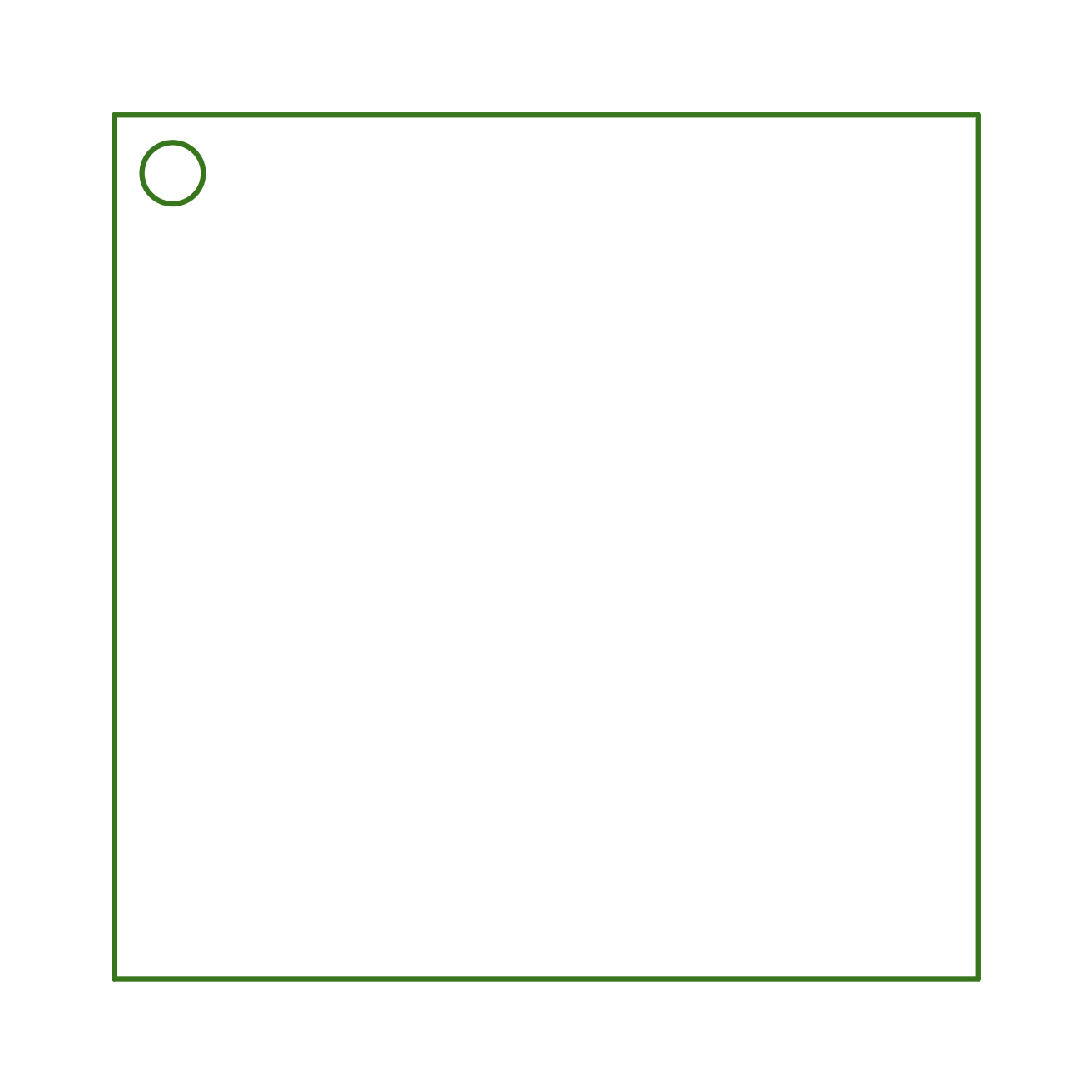
IC package outlines include one pin 1 polarity mark with the following specifications:
-
Circle shape
-
Radius of 0.5 mm
-
Arc width of 0.1 mm
-
Position it inside the package outline, aligned with pad 1
-
-
The package outline should be a reasonable 2D representation of the component. The package outline line width must be 0.1 mm.
-
When working with memory connectors that have memory cards (e.g., SD Card) inserted, the package outline and the courtyard should represent the connector component only. Do not include the memory card placement outline on any layer.
-
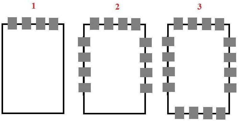
When the package outline dimension has tolerances, follow these instructions:
-
In Example 1, the left-right tolerance is divided equally on both sides, and the top-down tolerance goes completely to the bottom side. In Examples 2 and 3, the left-right tolerance is divided equally on both sides, and the top-down tolerance is divided equally on both sides.
-
If the component has multiple measurements with multiple tolerances:
In the following example, there are 10 mm ±0.5 mm and 2 mm ±0.5 mm. There is also a 0.8 mm ±0.5 mm. Because the tolerance ±0.5 mm is greater than 50% of 0.8 mm, it can be ignored. This is called the 50% rule.
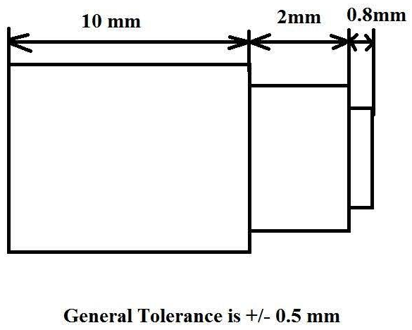
For this example, we will add the tolerance so the total = 10 mm + 0.5 mm + 2 mm + 0.5 mm + 0.8 mm = 13.8 mm.
-
In the rare case when the datasheet does not provide maximum dimensions or tolerances and only the nominal dimensions are available, use the nominal dimensions for the package outline calculation.
-
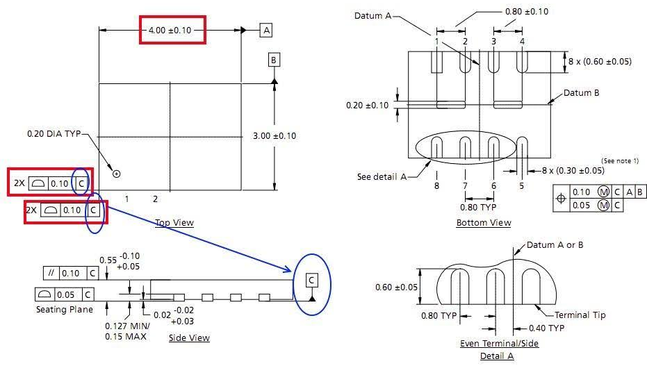
If the mechanical drawing indicates tolerance using the method below (half circle followed by a number and tolerance value in the measurement), use the tolerance value beside the measurement. In this case, only use the tolerance value included in the dimension - 0.1 mm. In the example below, Package Outline = 4.00 mm + 0.1 mm = 4.1 mm.
-
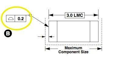
If the mechanical drawing indicates tolerance using the method below (half circle followed by a number), this indicates that the component can increase in either direction by 0.2/2 mm. Unless the dimension indicates LMC or MIN, in which case the component can increase in either direction by 0.2 mm. In the example below, the package outline length (Max Length) = 3.0 mm + 2 x 0.2 mm = 3.4 mm.
-
Top Component Dims
The Component Dims layer is used to define the dimensional detail required for components.
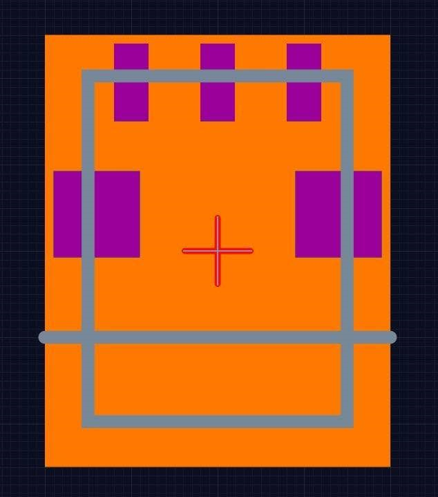
Note: For connectors that hang over the board edge, place a line that the PCB designer should use to align the connector to the board edge. The datasheet for such connectors generally has a recommended footprint that includes relative measurements from the board edge, so simply add a line to represent the board edge. Place this line on the Top Component Dims layer. The length of this line should be equal to the width of the courtyard.
The board edge line width should be 0.1 mm.
Top Solder
This guideline suggests defaulting to the 1:1 rule as a baseline, where the solder mask openings match the pad sizes exactly per IPC-7351B for all IPC-compliant components.
For the Recommended Land Pattern variant, if the component manufacturer recommends a different solder mask expansion, follow the component manufacturer's recommendation.
Top Paste
This guideline suggests defaulting to the 1:1 rule as a baseline, where the paste mask openings match the pad sizes exactly per IPC-7351B for all IPC-compliant components except for thermal pads.
For the Recommended Land Pattern variant, if the component manufacturer recommends a different paste mask expansion, follow the component manufacturer's recommendation.
Top Layer
-
For the recommended land pattern variant, the pad shapes should 100% match the shape indicated in the MFG recommended footprint.
-
For the recommended land pattern variant, the pad coordinates must exactly match the datasheet.
-
For the recommended land pattern variant, the pad sizes (width, length, rounding angle, etc.) must exactly match the datasheet.
-
For IPC-compliant footprints, the pad size and coordinates should be calculated per IPC-7351B equations with the following notes:
-
Table 3-2 through Table 3-22 indicate the round-off factor used for the three goals established by the IPC-7351B standard. The round-off factor could be 0.05 mm or 0.02 mm depending on the component family that share similar solder joint engineering goals.
-
For gull wing components where the minimum distance between component terminations is less than or equal to maximum package height, different heel fillet goals are followed based on IPC-7351B.
-
For components with a standoff height of less than 0.15 mm, care should be taken when determining the land pattern length for gull-wing leads. This is to prevent solder paste from extending under the package body, which could lead to solder bridging between leads due to the heel fillet. While trimming the pads may be necessary, the heel fillet should not be reduced below the IPC-7351B minimum requirement. For instance, components like Flat Ribbon L and Gull-Wing Leads with a pitch of ≤ 0.625 mm require a heel fillet of 0.25 mm for Level C density. Any trimming must ensure this minimum heel fillet is maintained.
-
The following formula is used to determine the BGA pad size:
BGA Pad Size = Nominal Ball Diameter x (1 ± %P) + (Maximum Land Variation Value - Nominal Land Diameter)
where P is the percentage adjustment; a reduction for collapsible balls and an increase for non-collapsible balls. The percentage, maximum land variation, and nominal land diameter values can be found in the following tables.Land Approximation (mm) for Collapsible Solder Balls Nominal Ball Diameter Reduction Nominal Land Diameter Land Variation 0.75 25% 0.55 0.60 - 0.50 0.65 25% 0.50 0.55 - 0.45 0.60 25% 0.45 0.50 - 0.40 0.55 25% 0.40 0.50 - 0.40 0.50 20% 0.40 0.45 - 0.35 0.45 20% 0.35 0.40 - 0.30 0.40 20% 0.30 0.35 - 0.25 0.35 20% 0.28 0.33 - 0.23 0.30 20% 0.25 0.25 - 0.20 0.25 20% 0.20 0.20 - 0.17 0.20 15% 0.17 0.20 - 0.14 0.17 15% 0.15 0.18 - 0.12 0.15 15% 0.13 0.15 - 0.10
Land Approximation (mm) for Non-Collapsible Solder Balls Nominal Ball Diameter Increase Nominal Land Diameter Land Variation 0.75 15% 0.85 0.80 - 0.90 0.60 15% 0.70 0.65 - 0.75 0.55 15% 0.65 0.60 - 0.70 0.50 10% 0.55 0.50 - 0.60 0.45 10% 0.50 0.45 - 0.55 0.40 10% 0.45 0.40 - 0.50 0.30 10% 0.33 0.28 - 0.38 0.25 10% 0.28 0.23 - 0.33 0.20 5% 0.21 0.18 - 0.24 0.17 5% 0.18 0.15 - 0.21 0.15 5% 0.16 0.13 - 0.19
-
-
For IPC-compliant footprints, the pad shape must be oblong or rounded.
Top Courtyard
-
Courtyard line width should be 0.05 mm.
-
For IPC-compliant footprints, this guideline suggests following the IPC-7351B standard when determining the courtyard excess or clearance. This standard is based on three density levels and the individual package types.
-
If the datasheets recommended land pattern suggests a courtyard, follow this recommendation.
-
If the datasheet recommended land pattern does not provide courtyard information, follow the IPC-7351B standard for determining the courtyard excess or clearance for the recommended land pattern variant.
-
If the datasheet indicates a component keepout that is larger than the calculated courtyard, follow the datasheet and make the courtyard equal to the datasheet component keepout.
Top Silkscreen
-
The silkscreen outline should be designed following the maximum package outline with an offset towards the outside of the package outline of one half of the silkscreen line width. For example, if the silkscreen line width is 0.127 mm, then the silkscreen line is 0.0635 mm offset from the package outline line.
-
Silkscreen should be a minimum of 0.2 mm away from any exposed copper.
-
Silkscreen line width should be 0.127 mm.
-
The silkscreen legend should never be underneath the component body for SMD packages.
-
If the clearance guideline mentioned previously cannot be met for small packages such as 01005, there is no silkscreen outline. For larger packages, the silkscreen outline can be a short line or even a dot.
-
The silkscreen guideline applies to all IPC density levels.
-
Legend polarity mark is required on the silkscreen layer. Polarity marks should maintain a minimum space of 0.177 mm between the edge of the polarity mark and the edge of any copper pad. This will allow for solder mask expansions from 0.0 mm up to 0.10 mm and still maintain the minimum IPC spacing for silkscreen to solder mask opening. Some recommendations are outlined in the table below.
Table 13. Legend Polarity Mark Examples Component Type Polarity Mark Location Polarity Mark Shape Polarity Mark Size Graphic Example Battery Next to the positive terminal. "+" sign 1.0 mm x 1.0 mm, 0.127 mm line width 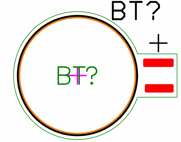
Diode/LED Above the cathode pad and even with the outer edge of the cathode pad. It must remain outside of the package outline. Open Triangle 0.19 mm x 0.38 mm, 0.127 mm line width 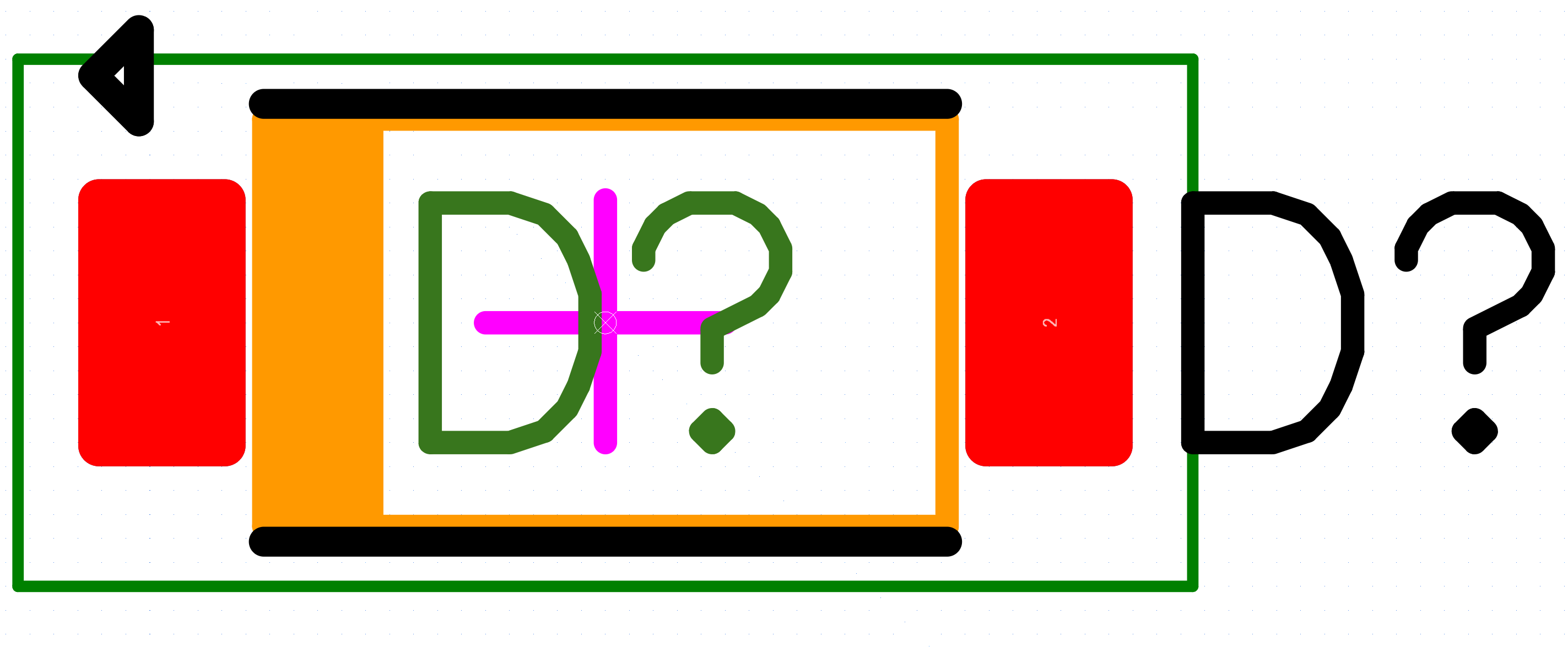
IC Above the end of pad 1 and even with the outer edge of pad 1. It must remain outside of the package outline. Dot Diameter of 0.25 mm for packages 5 mm x 5 mm or smaller
Diameter of 0.50 mm for packages larger than 5 mm x 5 mm
Polarized Capacitor Along the end of the positive pad, following the length of the pad. Line 0.127 mm line width 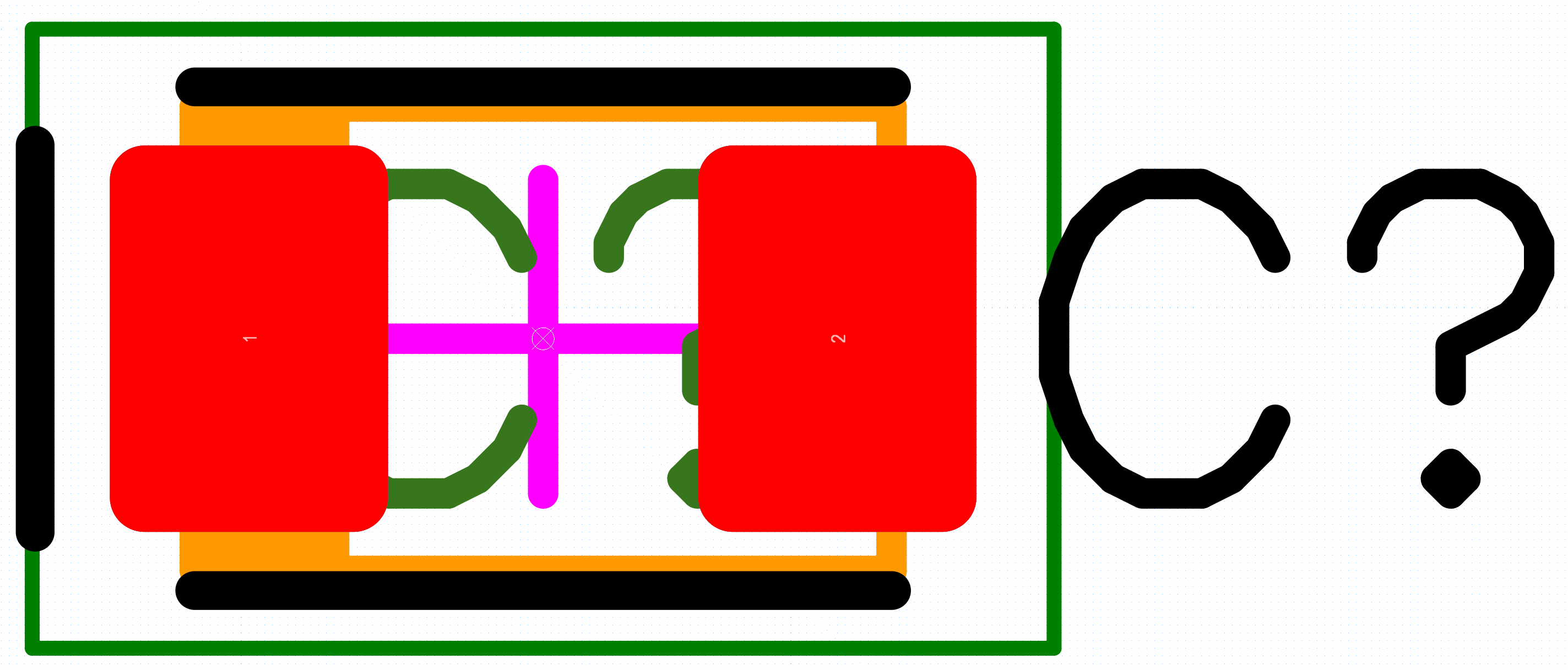
Polarized Inductor Along the end of the positive pad, following the length of the pad. Line 0.127 mm line width 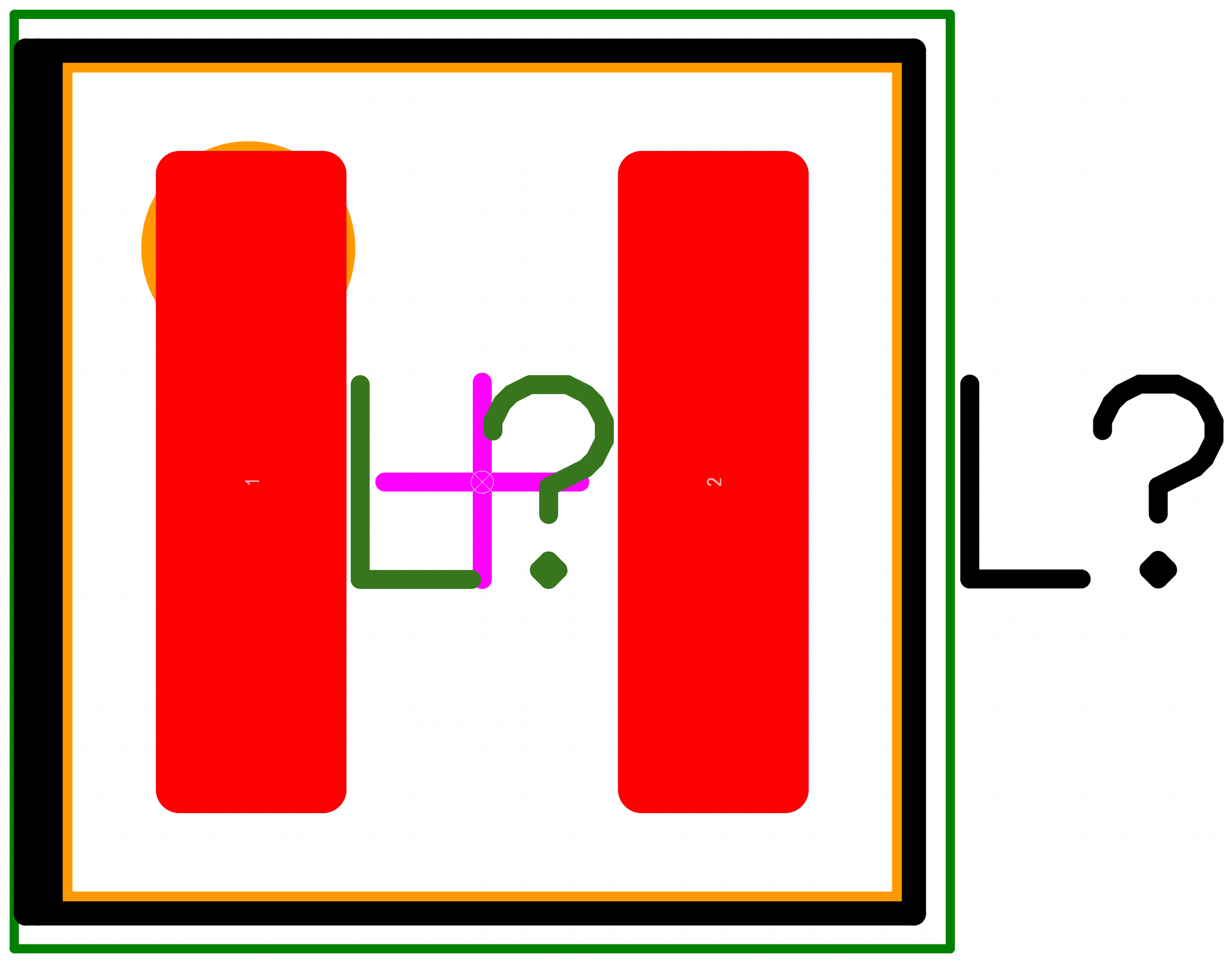
-
When a polarized component has an anode or negative pin polarity mark on its package, add the polarity mark shape on the right side by Pad 2.
-
If there is a fixed distance to the board edge in the recommended land pattern or the mechanical drawing, always, place the silkscreen 0.5 mm of the board edge line and no silkscreen past the board edge line.
-
If the component can be either fully placed within the board outline or hung partially off the board edge, design the silkscreen as if it were going to be placed fully on the board.
Keep-Out Layer
The keepout layer defines the areas used to prevent any or selected copper objects from being placed within them.
If the datasheet shows a keepout area, follow the datasheet’s drawing to design the keepout object. Some components, such as antennas, connectors and wireless modules, specify a keepout region.
Bottom Layer
Some footprints, such as board edge connectors, require copper on the bottom layer. If the component calls for pads or other copper items on the bottom of the board, it must be added to this layer.
Top Designator
A reference designator should be placed at the footprint origin. The designator should follow these recommendations:
-
Text Height is 1 mm.
-
Center justified.
-
Layer Top Designator.
Other Layers
Some footprints may use other layers, such as bottom paste, bottom solder, bottom silkscreen, etc. Use the same guidelines described for top layers.
Layer Usage
This guide recommends the following layers be used to create a footprint and support the footprint in a PCB design. Experience has shown that the essential layers provide the best flexibility for PCB design, documentation, and fabrication and assembly output. The essential layers are required footprint layers; the optional layers provide additional capability and flexibility as needed. Typically, only the top layers are used for footprint creation, but bottom layers may be used. Both top and bottom layers are usually required in the PCB design.
| Component Related Layers | ||
|---|---|---|
| Essential | TOP LAYER | Place the land pattern on this layer. |
| Essential | BOTTOM LAYER | |
| Essential | TOP SOLDER | Place the solder mask opening definitions on this layer. |
| Essential | BOTTOM SOLDER | |
| Essential | TOP PASTE | Place the solder paste stencil opening definitions on this layer. |
| Essential | BOTTOM PASTE | |
| Essential | TOP SILKSCREEN | Place silkscreen or legend on this layer including reference designator and polarity marking if needed. |
| Essential | BOTTOM SILKSCREEN | |
| Essential | TOP ASSEMBLY | Detail the component package outline for assembly documentation. |
| Essential | BOTTOM ASSEMBLY | |
| Essential | TOP DESIGNATOR | Place a reference designator on this layer for documentation purposes. |
| Essential | BOTTOM DESIGNATOR | |
| Essential | TOP 3D BODY | Place the 3D model on this layer. |
| Essential | BOTTOM 3D BODY | |
| Essential | TOP COURTYARD | Place the courtyard on this layer. |
| Essential | BOTTOM COURTYARD | |
| Essential | TOP COMPONENT CENTER | Place the component center marker on this layer. |
| Essential | BOTTOM COMPONENT CENTER | |
| Optional | TOP VALUE | Place the value or part number on this layer if needed. |
| Optional | BOTTOM VALUE | |
| Optional | TOP COMPONENT OUTLINE | Define the area the component occupies on the board if needed. |
| Optional | BOTTOM COMPONENT OUTLINE | |
| Optional | TOP COMPONENT DIMS | Define the dimensional detail required for components if needed. |
| Optional | BOTTOM COMPONENT DIMS | |
| Optional | TOP GOLD PLATING | Define component selective gold plating requirements if needed. |
| Optional | BOTTOM GOLD PLATING | |
| Optional | TOP GLUE | Define the component assembly glue points if needed. |
| Optional | BOTTOM GLUE | |
| Optional | TOP CONFORMAL COAT | Define the component assembly conformal coating details if needed. |
| Optional | BOTTOM CONFORMAL COAT | |
| Optional | COMPONENT CAVITY | Define the embedded component cavity definition if needed. |
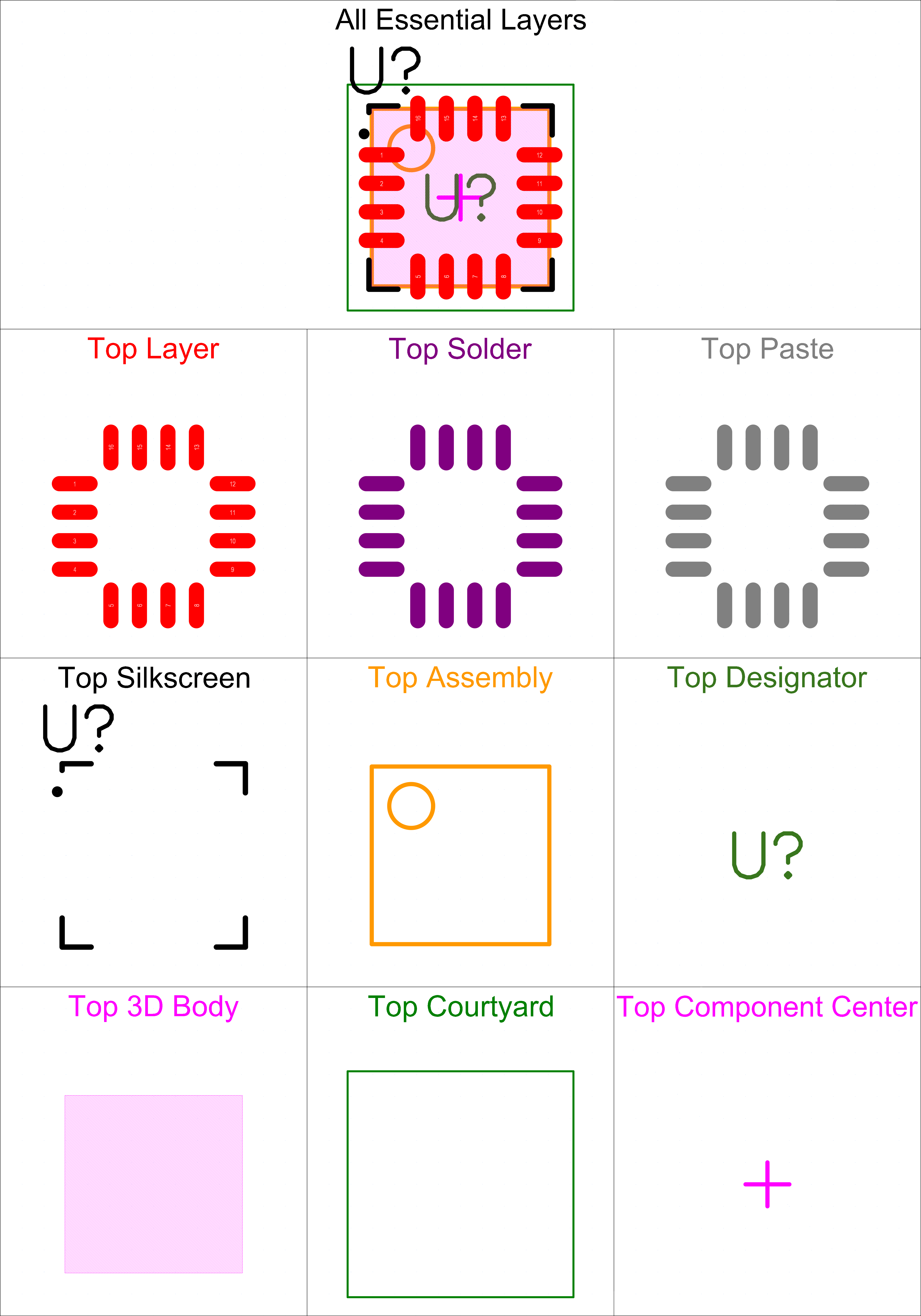
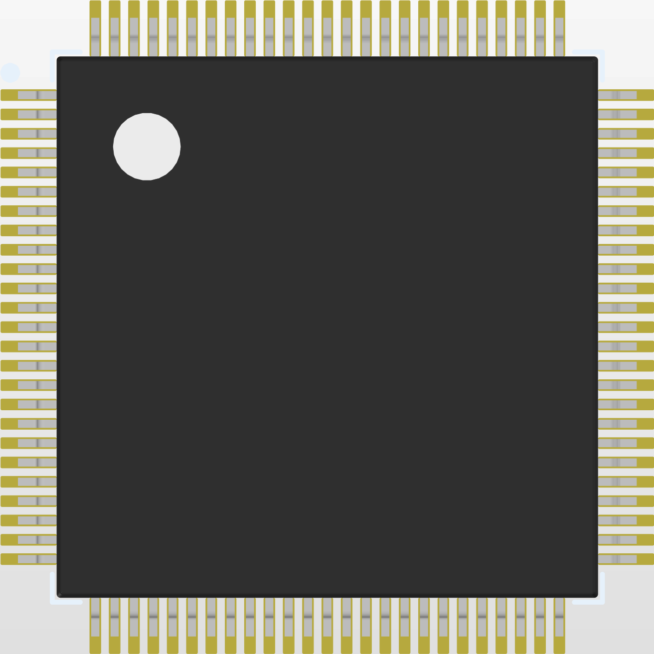
It is important to note the difference between the Top and Bottom Assembly layers and the Top and Bottom Component Outline layers. The Top and Bottom Assembly layers are used to represent the component package outline drawn to maximum dimensions, typically used for assembly documentation. The Top and Bottom Component Outline layers are used to represent the total area on the board occupied by the component.
| 3D Body | Top Assembly | Top Component Outline |
|---|---|---|
 |
 |
 |