This section provides information to enhance schematic symbol, PCB footprint and 3D model design clarity and consistency within Altium Designer. These recommendations include considerations for pin organization, pin symbols, pin functions, parameters and more. It also covers some best practices for footprint creation and component labeling.
Parameters in Altium Designer
Component Parameters can be added in Altium Designer from the component library source. Schematic library parameters can be added with a schematic component library document open, using the properties panel. There are special purpose component parameters: HelpURL parameter and Link parameters.
HelpURL Parameter
The value of this parameter is the most reliable URL link to the datasheet. The HelpURL parameter is unique to Altium Designer and should be used as the primary link to the datasheet source. It is designed to provide instant access to a component’s datasheet using the F1 help key in the Altium Designer schematic editor.
Any component models created for use in Altium Designer should have the HelpURL parameter in the component’s parameter list.
When viewing a schematic in Altium Designer, with the cursor anywhere that is not over a component symbol, pressing the F1 key opens the Altium online documentation for the schematic editor. However, if the cursor is hovering over a symbol and the F1 key is pressed, Altium looks for the HelpURL parameter in that symbol’s parameter list. If the HelpURL parameter is there, Altium instantly launches the link in the value of the HelpURL parameter. This feature allows a schematic user to quickly access a component’s datasheet by simply pressing the F1 key when the mouse cursor is hovering over the component symbol.
Link Parameters
The Links feature in Altium Designer enables the definition and presentation of named links to any number of reference URLs or documents, for example, manufacturer’s product catalog, manufacturer's product page, manufacturer’s package drawing and manufacturer's recommended land pattern.
When creating a symbol in the symbol editor in Altium Designer, the Links can be added to the symbol in the parameters section of the component properties.
Symbol Pin Functions
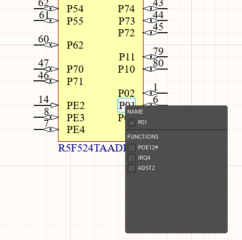
In Altium Designer, you can program pin names into parts and choose pin configurations directly on a schematic sheet. When naming multi-functional pins, use the pin name (function upon reset) or the first function listed in the pin name list.
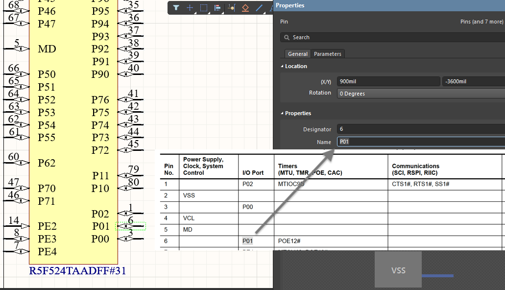
Additional or alternate functions can be added in the pin properties under "Function."
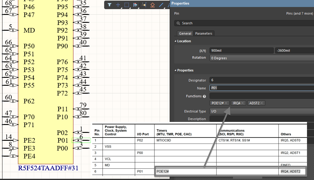
On the schematic, you can then select the desired pin function.
Pin Symbols
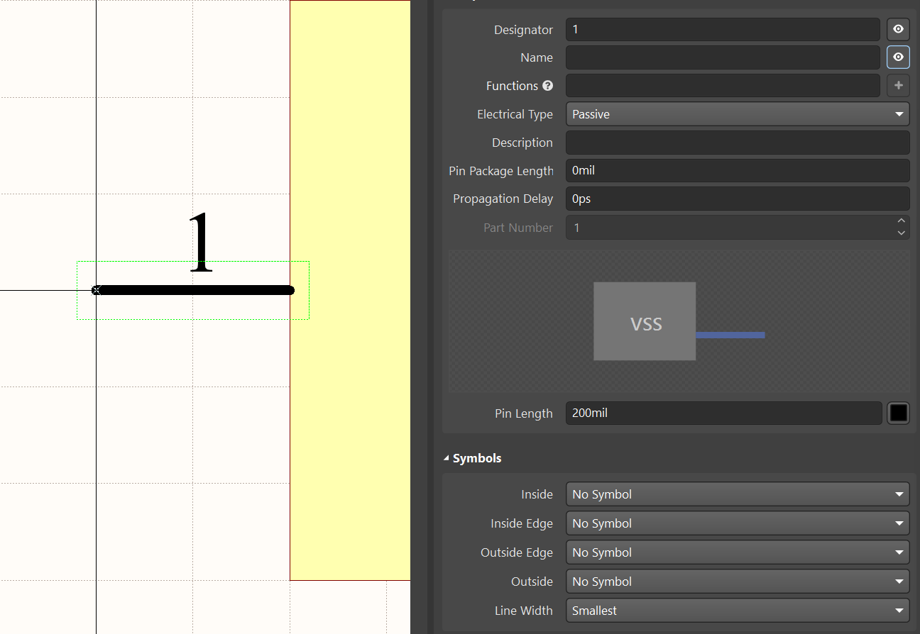
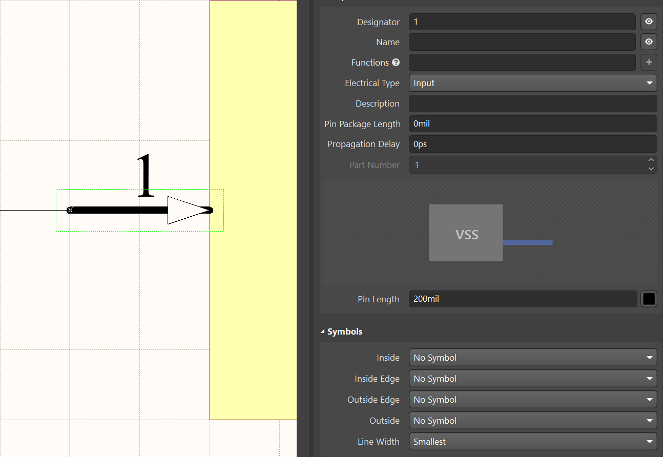
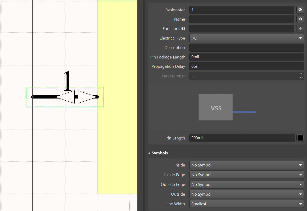
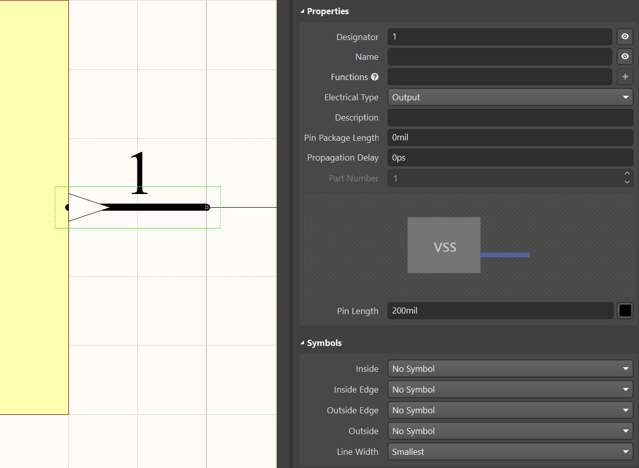
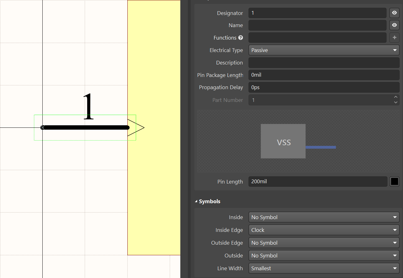
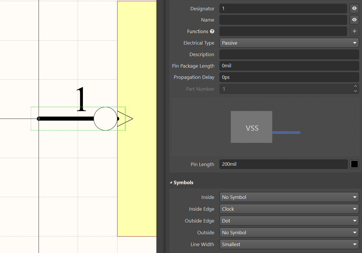
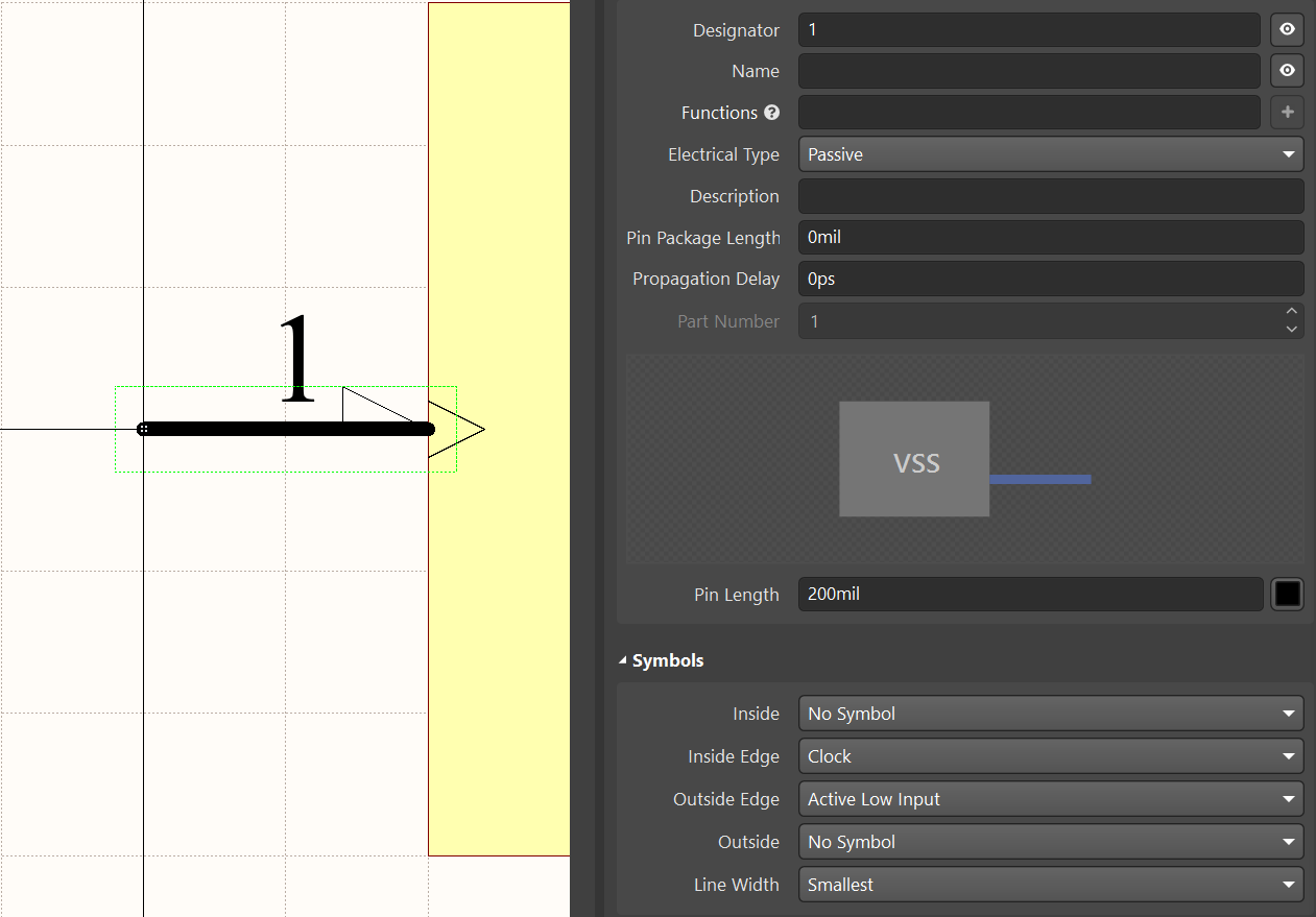
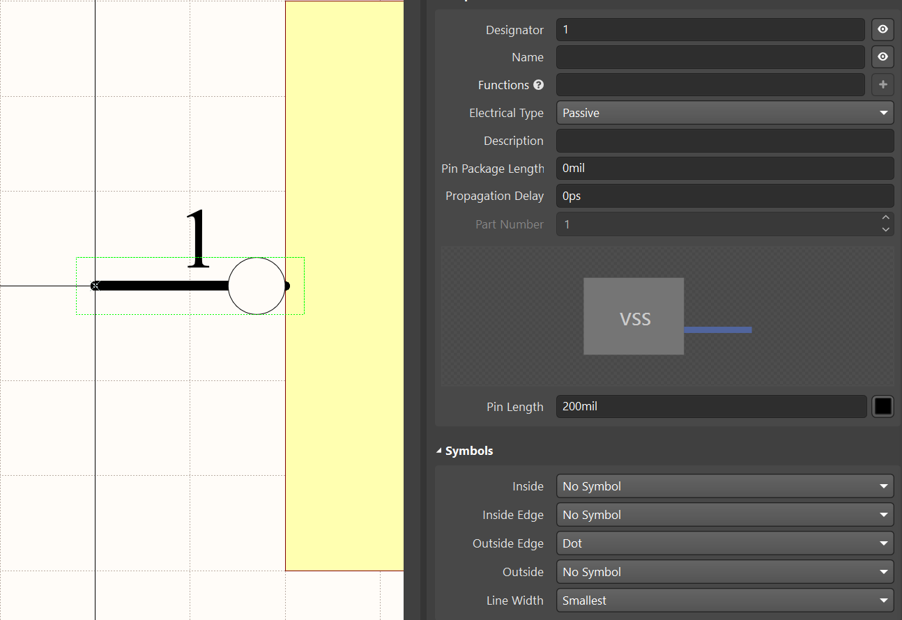
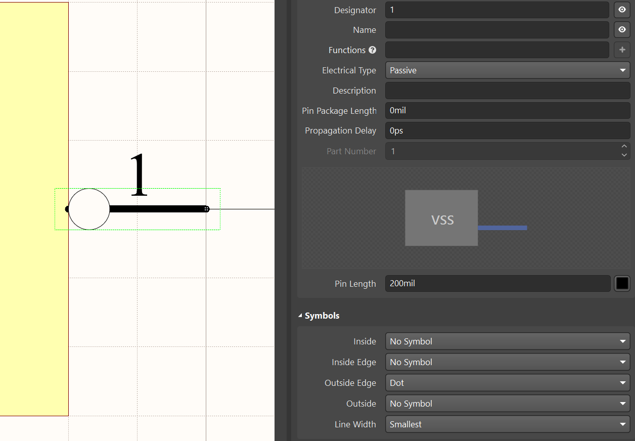
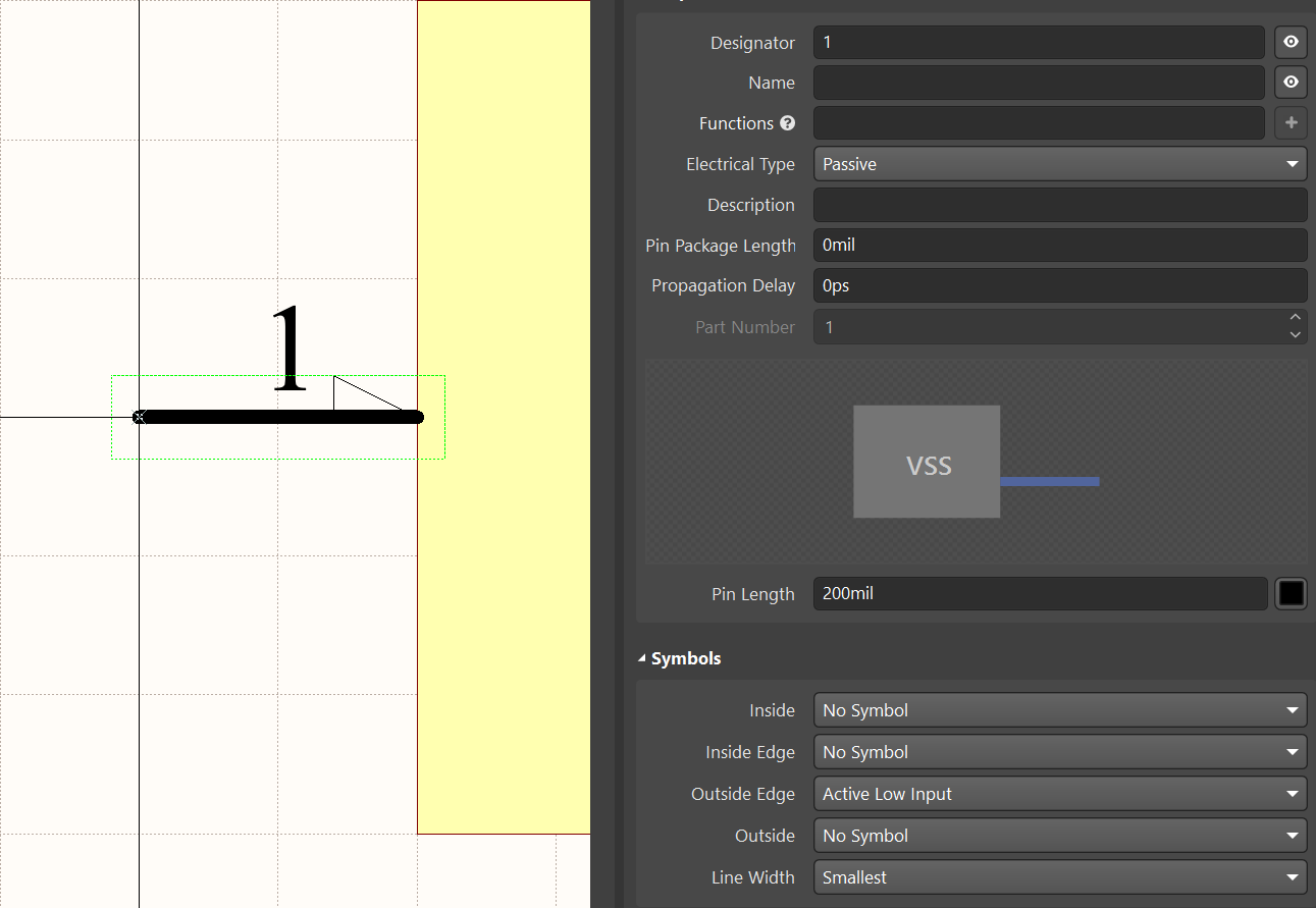
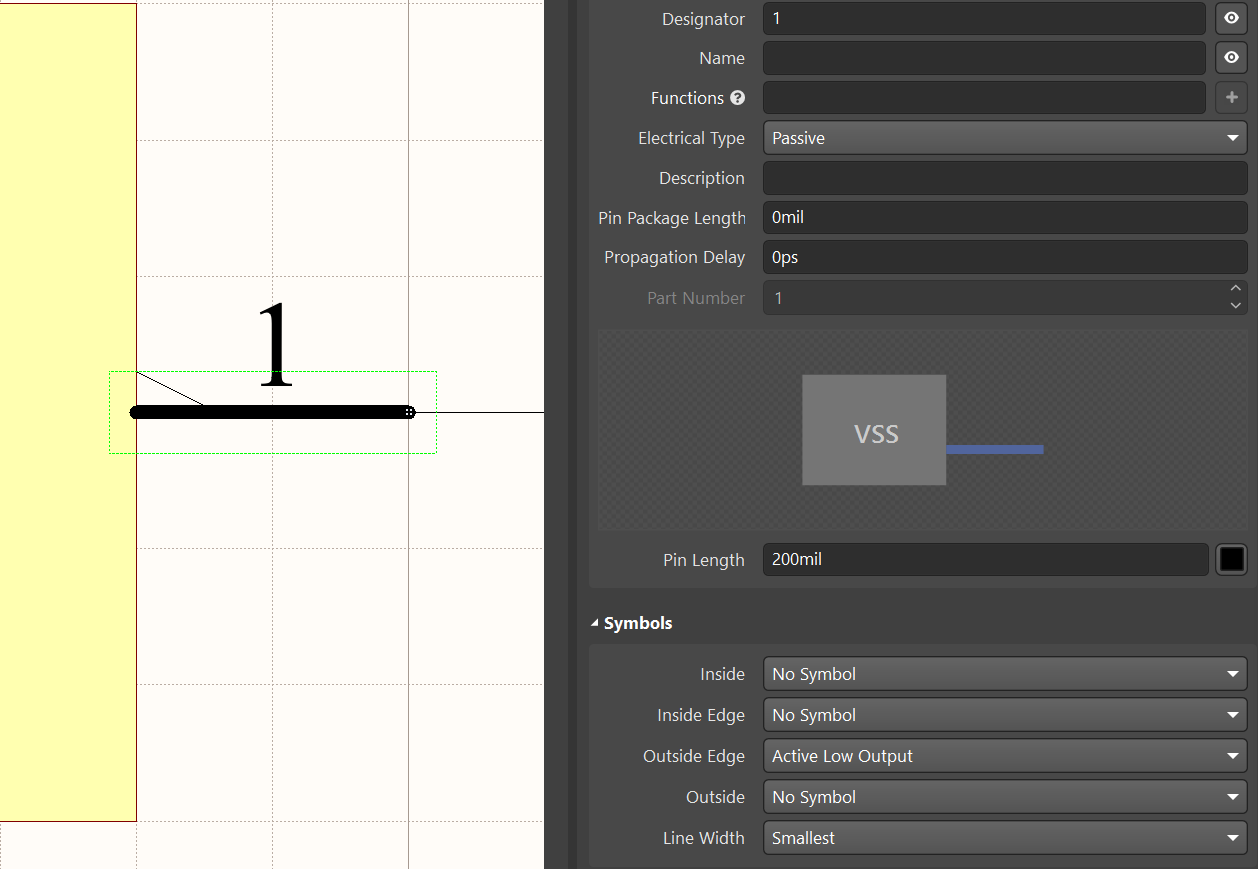
To aid in the interpretation of individual signals it is suggested to use Pin Symbols. Some of the most commonly used pin symbols available in Altium Designer are listed below. This list is not exhaustive. Pin symbols are assigned in Altium Designer by selecting an electrical type from the Electrical Type drop-down list in the Properties panel with the pin selected. Then, optionally, selecting a symbol or combination of symbols from one or more of the five drop-down lists in the "Symbols" section of the pin properties.
-
Passive Pin: This is a common general pin symbol.
-
Input Pin: This is a common Input pin symbol.
-
I/O Pin: This is a common I/O pin symbol.
-
Output Pin: This is a common Output pin symbol.
-
Clock Pin: This is a Clock pin symbol. Transition up from 0 to 1 for Positive Logic. Transition down from 0 to 1 for Negative Logic. Transition from Low to High for Polarity Indication per IEEE Standard 91-1984.
-
Clock Pin with Logic Negation at Input: This is a Clock with Logic Negation pin symbol. Transition down from 1 to 0 for Positive Logic. Transition up from 1 to 0 for Negative Logic. This pin symbol should not be used for Polarity Indication per IEEE Standard 91-1984.
-
Clock Pin with High to Low Polarity Indication: This is a Clock with High to Low Polarity Indication pin symbol. This symbol should not be used for Positive or Negative Logic. Use this symbol for transition from High to Low Polarity Indication per IEEE Standard 91-1984.
-
Logic Negation at Input: This is a Logic Negation Input pin symbol. External 0 produces internal 1.
-
Logic Negation at Output: This is a Logic Negation Output pin symbol. Internal 1 produces external 0.
-
Active-Low Input: This is an Active-Low Input pin symbol. Equivalent to Logic Negation at Input (above) for Positive Logic per IEEE Standard 91-1984.
-
Active-Low Output: This is an Active-Low Output pin symbol. Equivalent to Logic Negation at Output (above) for Positive Logic per IEEE Standard 91-1984.
Reference Designator in Altium Designer
If the reference designator is not placed at the symbol design level, and if the reference designator Autoposition property is checked (the reference designator's Autoposition property is checked by default), Altium Designer will place the reference designator above and to the left of the symbol graphics when the symbol is placed at the schematic level.
Footprint Considerations in Altium Designer
-
Pad Shape: In Altium Designer, oblong pad shapes are round pad shapes, and rounded pad shapes are rounded rectangle pad shapes.
-
Paste Mask: In Altium Designer, set the paste mask expansion to a negative number (half the length of the shortest side of the thermal pad) to make the paste of the pad disappear. Create a set of regions on the paste layer for the array and place them evenly over the thermal pad.
-
Top Silkscreen:
-
If the datasheet does not have a dimension and a 3D model is available, it is recommended to use 3D model snap points in Altium Designer to help position the 3D model and help draw the package outline.
-
The reference designator in the silkscreen layer is automatically assigned in Altium Designer, and does not need to be placed in the footprint.
-
-
Top Designator: place a .Designator special string at the footprint origin on the top designator layer. The .Designator string should follow these recommendations:
-
Text Height is 1 mm.
-
Font Type is Stroke.
-
Justification is Center, Center.
-
Font is Sans Serif.
-
Stroke Width is 0.1 mm.
-
Layer Top Designator (Mechanical 11).
-
Layers in Altium Designer
The following Altium layer mapping is suggested as a standard. This mapping includes the Layer Type settings available in the Edit Layer dialog in Altium Designer for both single mechanical layers as well as for layer pairs. When there are two consecutive similar layers where the first layer begins with TOP…, and the next layer begins with BOTTOM…, these two layers should be used to create a corresponding layer pair in Altium Designer. For example, Mechanical Layer 9, TOP GLUE, and Mechanical Layer 10, BOTTOM GLUE, would be used to create a Layer Pair called GLUE with the Layer Type setting set to Glue Points.
Layer Types make it easier to share Altium Designer data when different layer numbers have been used for the same layer information by different users. For example, one uses Mechanical Layers 13 and 14 for Top and Bottom 3D Bodies, and the other uses Mechanical Layers 14 and 15 for Top and Bottom 3D bodies. 3D body data could potentially be lost when sharing between the two users. However, if both users have assigned the Layer Type of the 3D body to their respective 3D body layer pair, then when loading data from each other, the 3D body data will be mapped to the corresponding layer numbers that match the Layer Type. See Working with Mechanical Layers” in the Altium Designer online documentation for more information.
This layer mapping also includes some basic layers needed for Flex and Rigid-Flex PCB designs.
| 1-8 Board Related Layers | ||
| Mechanical 1 | BOARD SHAPE | Overall board outline or profile - Layer Type = Board Shape |
| Mechanical 2 | ROUTE TOOL PATH | Mechanical routing information - Layer Type = Route Tool Path |
| Mechanical 3 | DIMENSIONS | Dimensional detail required for the board - Layer Type = Dimensions |
| Mechanical 4 | HOLE DETAIL | Dimensional detail required for special holes |
| Mechanical 5 | DXF IMPORT | Mechanical details imported from DXF |
| Mechanical 6 | V-CUT | V-Groove or scoring details - Layer Type = V Cut |
| Mechanical 7 | BOARD | Detail board-related instructions or details - Layer Type = Board |
| Mechanical 8 | User defined | |
| 9-33 Component Related Layers | ||
| Mechanical 9 | TOP ASSEMBLY | Detail component package outline for assembly - Layer Type = Assembly *Can be used by Draftsman |
| Mechanical 10 | BOTTOM ASSEMBLY | |
| Mechanical 11 | TOP DESIGNATOR | .Designator special string layer pair - Layer Type = Designator |
| Mechanical 12 | BOTTOM DESIGNATOR | |
| Mechanical 13 | TOP 3D BODY | 3D model layer pair - Layer Type = 3D Body |
| Mechanical 14 | BOTTOM 3D BODY | |
| Mechanical 15 | TOP COURTYARD | Component required placement space layer pair - Layer Type = Courtyard |
| Mechanical 16 | BOTTOM COURTYARD | |
| Mechanical 17 | TOP COMPONENT CENTER | Indicate the centroid of the component - Layer Type = Component Center |
| Mechanical 18 | BOTTOM COMPONENT CENTER | |
| Mechanical 19 | TOP VALUE | Place the .Comment special string - Layer Type = Value |
| Mechanical 20 | BOTTOM VALUE | |
| Mechanical 21 | TOP COMPONENT OUTLINE | Define the area the component occupies on the board - Layer Type = Component Outline |
| Mechanical 22 | BOTTOM COMPONENT OUTLINE | |
| Mechanical 23 | TOP COMPONENT DIMS | Define the dimensional detail required for components - Layer Type = Dimensions |
| Mechanical 24 | BOTTOM COMPONENT DIMS | |
| Mechanical 25 | TOP GOLD PLATING | Define component selective gold plating requirements - Layer Type = Gold Plating |
| Mechanical 26 | BOTTOM GOLD PLATING | |
| Mechanical 27 | TOP GLUE | Component assembly glue points layer pair - Layer Type = Glue Points |
| Mechanical 28 | BOTTOM GLUE | |
| Mechanical 29 | TOP CONFORMAL COAT | Component assembly conformal coating details layer pair - Layer Type = Coating |
| Mechanical 30 | BOTTOM CONFORMAL COAT | |
| Mechanical 31 | COMPONENT CAVITY | Embedded component cavity definition |
| Mechanical 32 | User defined | |
| Mechanical 33 | User defined | |
| 34-40 Board Documentation Related Layers | ||
| Mechanical 34 | FABRICATION NOTES | Detail important fabrication notes - Layer Type = Fab Notes |
| Mechanical 35 | ASSEMBLY NOTES | Detail component load order and/or important assembly notes - Layer Type = Assembly Notes |
| Mechanical 36 | TITLE BLOCK | Detail the drawing title block and sheet border - Layer Type = Sheet |
| Mechanical 37 | TITLE BLOCK MIRRORED | Detail a mirrored version of the drawing title block and sheet border |
| Mechanical 38 | CONTINUATION BLOCK | Detail a simplified drawing title block and sheet border for sheet(s) 2-n |
| Mechanical 39 | CONTINUATION BLOCK MIRRORED | Detail a mirrored version of the simplified drawing title block and sheet border for sheet(s) 2-n |
| Mechanical 40 | User defined | |
| 41-48 Panel Documentation Related Layers | ||
| Mechanical 41 | PANEL DIMENSION | Detail important panel layout dimensions |
| Mechanical 42 | PANEL FABRICATION NOTES | Detail important panel fabrication notes |
| Mechanical 43 | PANEL ASSEMBLY NOTES | Detail important panel assembly notes |
| Mechanical 44 | PANEL TITLE BLOCK | Detail the panel drawing title block and sheet border |
| Mechanical 45 | PANEL TITLE BLOCK MIRRORED | Detail a mirrored version of the panel drawing title block and sheet border |
| Mechanical 46 | PANEL CONTINUATION BLOCK | Detail a simplified drawing title block and sheet border for sheet(s) 2-n |
| Mechanical 47 | PANEL CONTINUATION BLOCK MIRRORED | Detail a mirrored version of the simplified drawing title block and sheet border for sheet(s) 2-n |
| Mechanical 48 | User defined | |
| 49-53 Flex and Rigid-Flex Related Layers | ||
| Mechanical 49 | TOP PSA | Define areas requiring pressure sensitive adhesive necessary for final assembly |
| Mechanical 50 | BOTTOM PSA | |
| Mechanical 51 | TOP STIFFENER | Define areas requiring a stiffener |
| Mechanical 52 | BOTTOM STIFFENER | |
| Mechanical 53 | BEND LINES | Detail flex bend lines |
Altium Designer Component Labeling
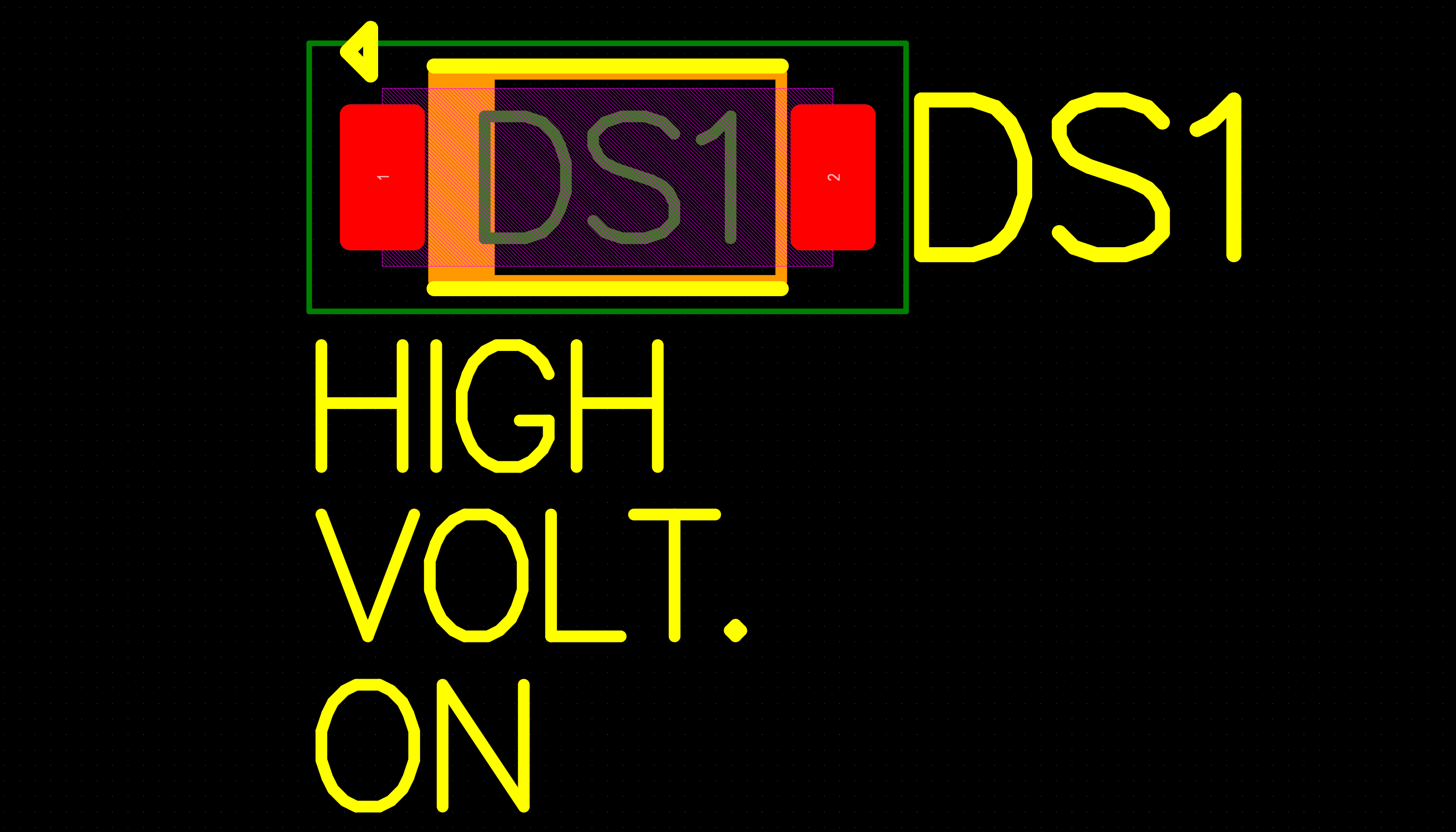
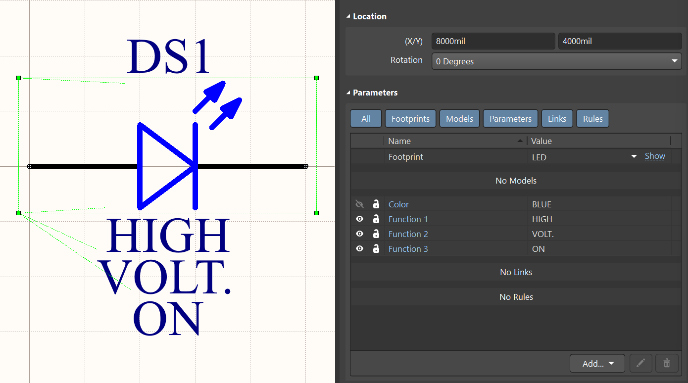
It can sometimes be very helpful to label some components to indicate a component’s function both in the schematic and on the printed circuit board’s legend. Components such as LEDs, switches, connectors and others have a specific human interface function that is helpful to make clear with a brief label. Although the following example is a good way to do it in Altium Designer, most electronic computer aided design applications provide this functionality in various ways.
In Altium Designer, component labels can be created using user-defined parameters. If these parameters are defined as described here they can always be there for use whether the labels are used or not. The user-defined label parameters must be included in the schematic symbol, as “special strings” on the Top Overlay layer in the footprint, and defined in the component’s parameters list for database or Workspace libraries.
Component Level Label Parameters
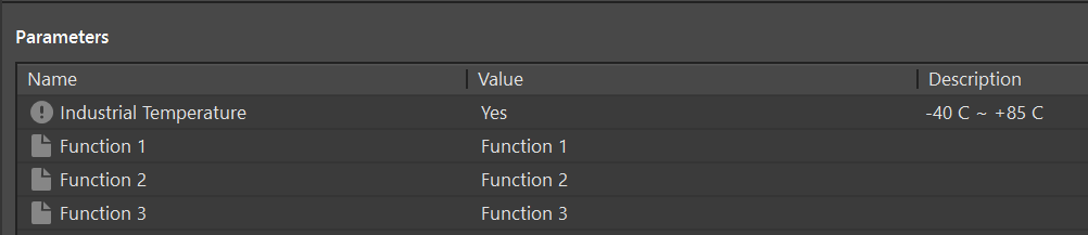
In the component define a set of user-defined parameters. This example will use user-defined parameters named ‘Function n' with a value of ‘Function n’, where n represents the number of user-defined parameters needed. It is recommended that at least three user-defined parameters be used to allow for maximum flexibility in placing them as labels on the legend or overlay layer in the PCB layout. In this example there are three user-defined parameters for use as labels in the schematic and on the PCB. They are Function 1 with a value of Function 1, Function 2 with a value of Function 2, and Function 3 with a value of Function 3. The values are placeholders. The actual values are defined by the end user at the time the component is placed in a schematic design.
Symbol Level Label Parameters
In the symbol define a set of user-defined parameters following the exact same naming and value conventions as used at the component level as shown above. Place these parameters at default locations near the symbol graphics and make them visible in the symbol’s parameters list.
Footprint Level Label Parameters
In the footprint place a set of special strings using the Place Text String feature on the Top Overlay layer. It is considered a ‘special string’ by using a period at the beginning of the text string. Altium Designer will replace the text in the special text string with the value of a parameter with the same name associated with the component. It may seem counterintuitive to place these special text strings in the middle of the component, but this is the best place to put them for two reasons. First, if the text strings are not used to label the component, they will become invisible as will be explained below. If they are invisible and are outside of the component area, there may be design rule check issues due to the invisible text strings. This is less likely to happen if the invisible strings are well within the component’s boundary. Second, if the text strings are used to label the component, they will always need to be moved into the best position for the label on a design by design basis.
Using Label Parameters
Once the schematic symbol, the footprint and component have the user-defined label parameters defined in them, and once the symbol and the footprint have been placed, managing the use of the label parameters is easy. If any label parameter is used, simply change the value of the parameter to how the label should read. It will display this way on the schematic. After the PCB is updated from the schematic, the label in the PCB will match the label in the schematic. If any label parameter is not needed, simply delete the value only. The label will disappear from the schematic and also will disappear from the PCB after updating from the schematic. To use a "not needed” label parameter again, simply place text for a label in the parameter’s value and it will show up on schematic and will be displayed on the board after it is updated from the schematic. This allows the schematic to control the labeling on the PCB automatically.
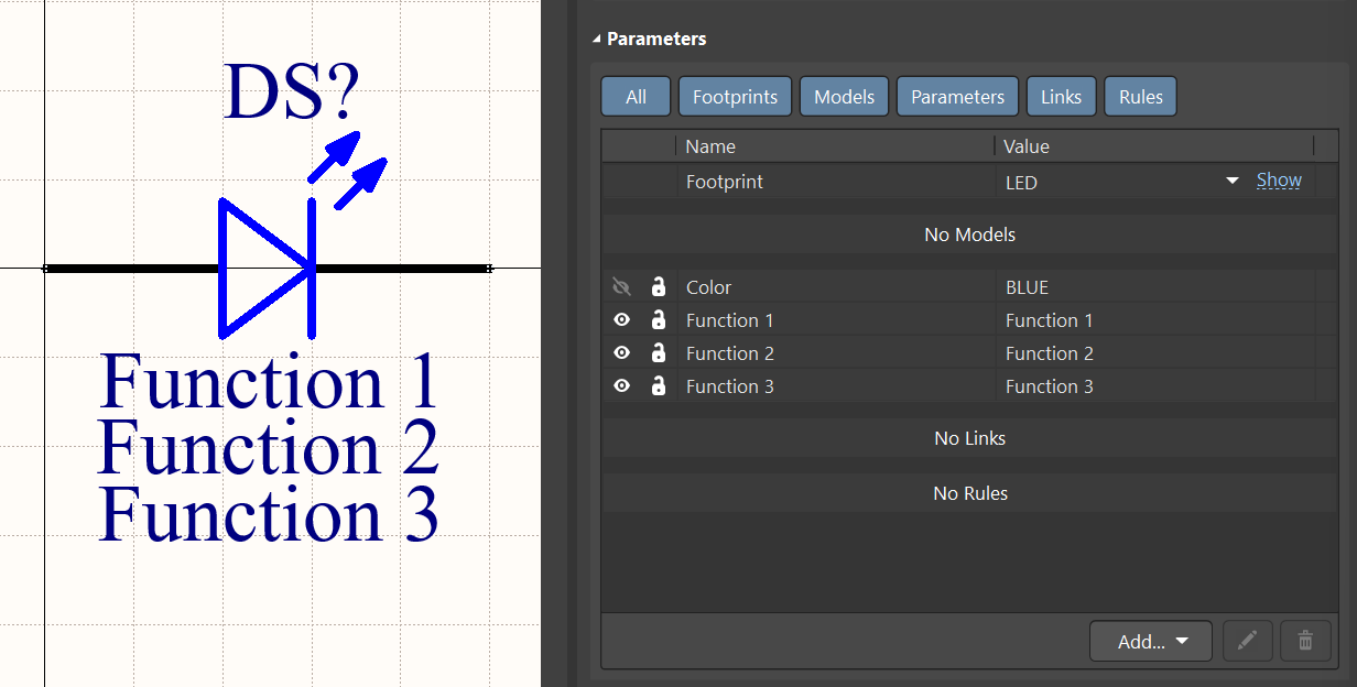
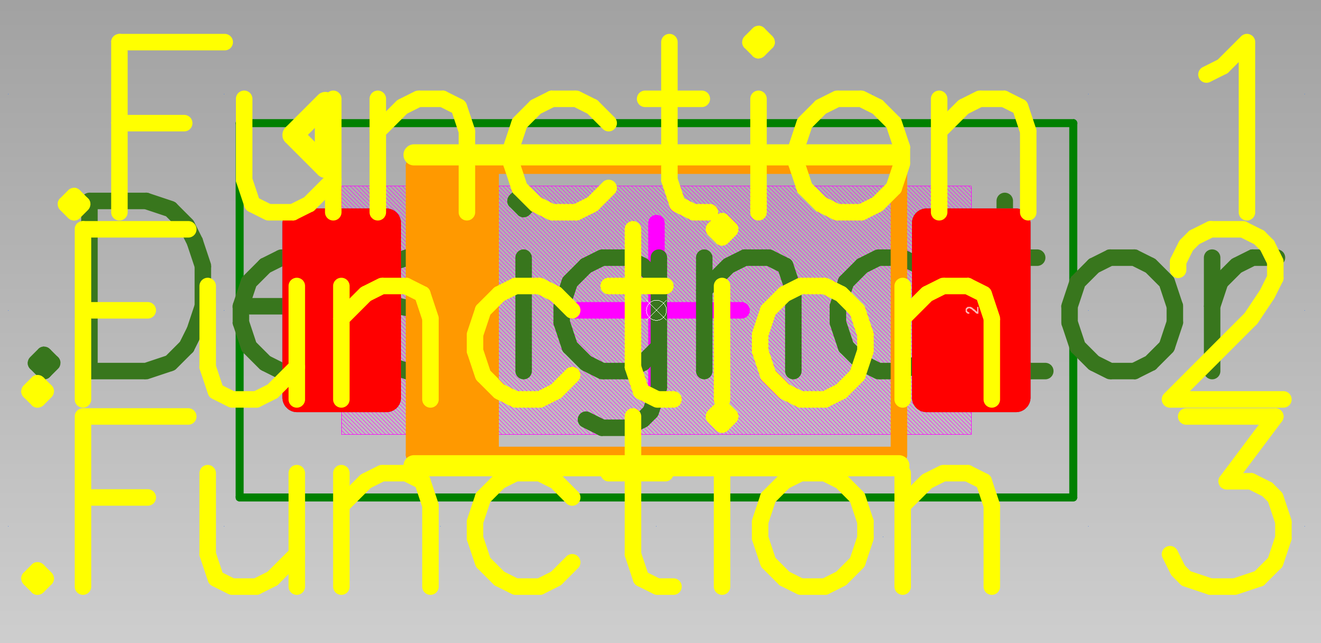
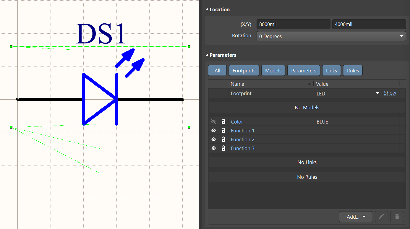
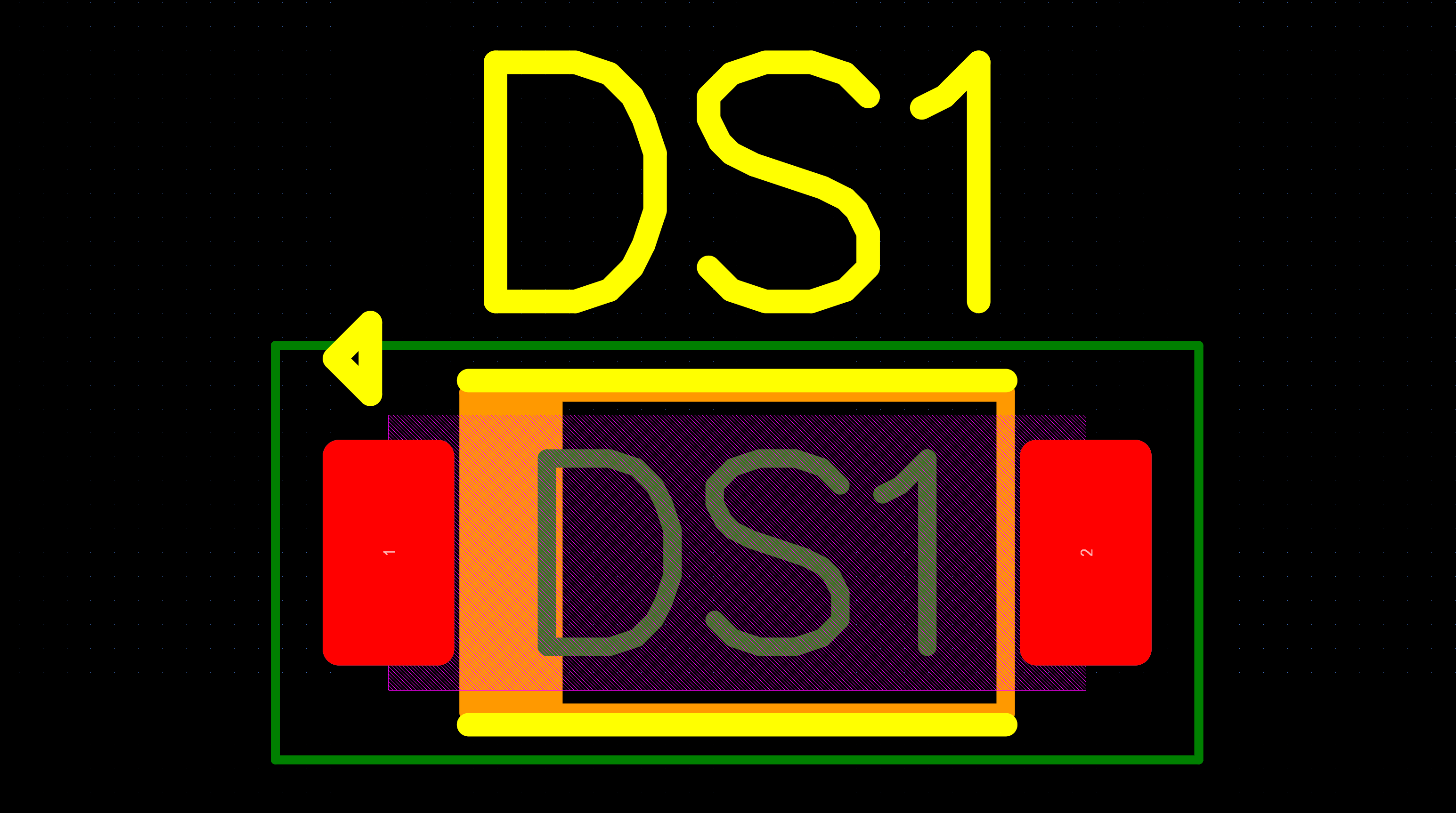
In the following example, the component has been placed in the schematic and the board has been updated. The label parameters still have the default placeholder values as originally defined in the library. The label parameter default values are displayed both on the schematic and on the PCB.
Schematic:
PCB:
In this next example, the labeling is not needed so the label parameters have their values deleted in the “Parameters” section of the Properties panel with the component selected. This makes them disappear from both the schematic and the PCB (after the PCB has been updated from the schematic).
Schematic:
PCB:
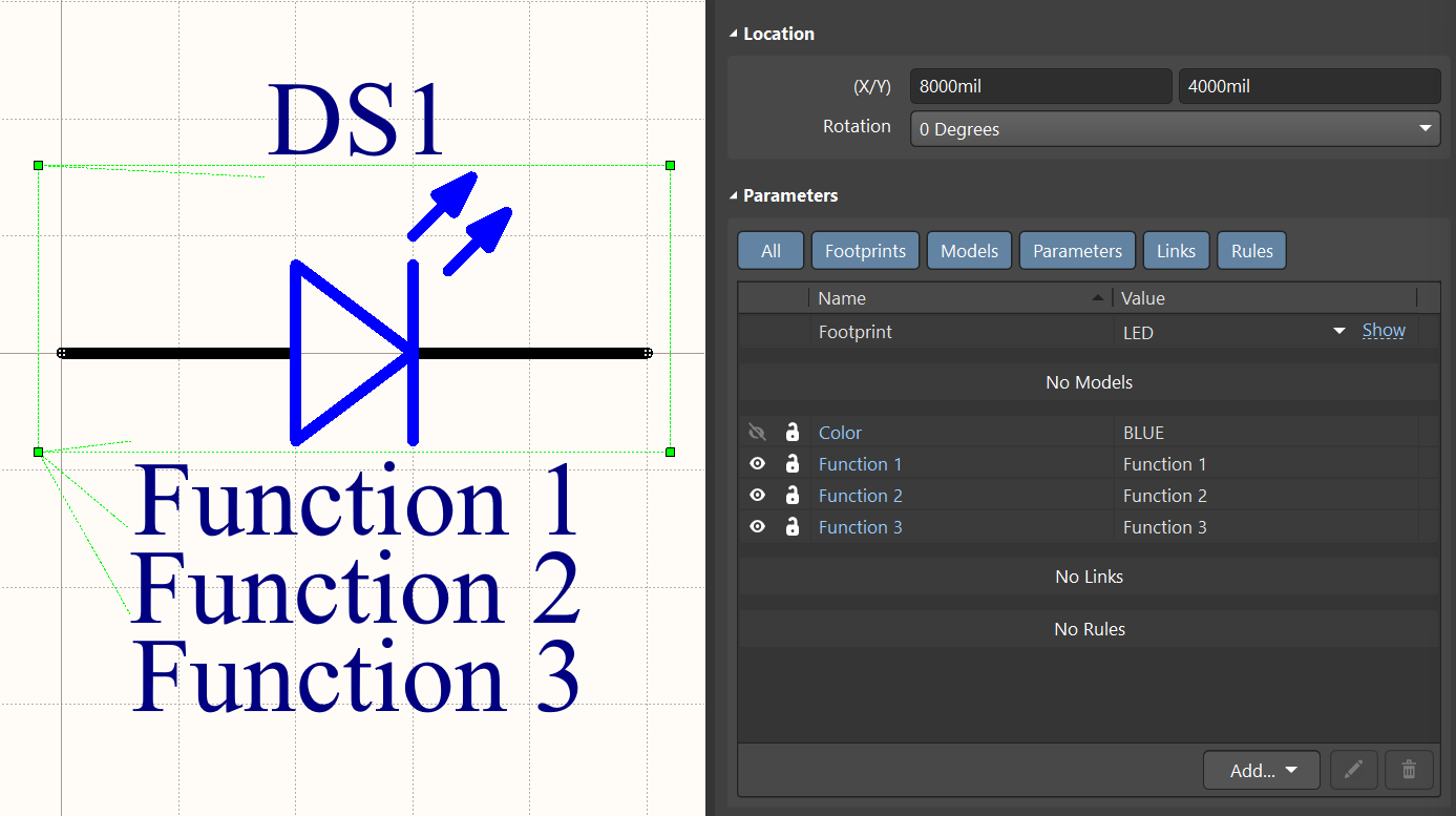
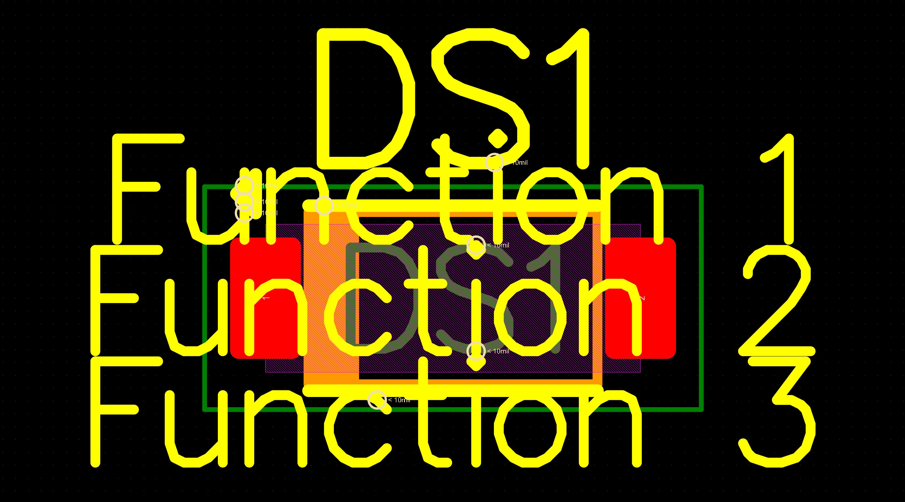
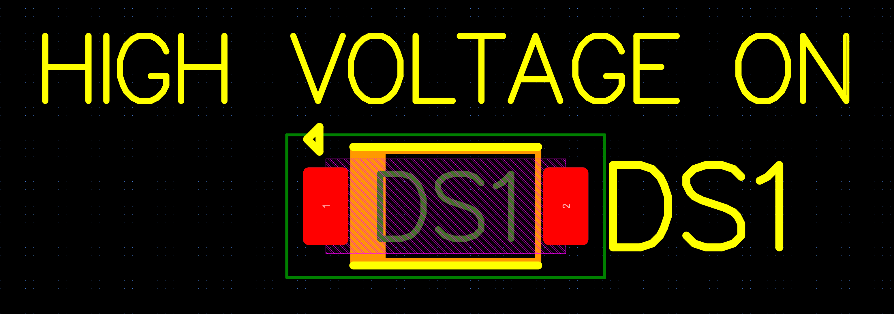
In this next example, only one label parameter is used while the other two label parameters are not used. Simply edit the label parameter values in the Properties panel with the component selected. Note the position of the reference designator and the position of the label parameter have been moved to a best location for the PCB design.
Schematic:
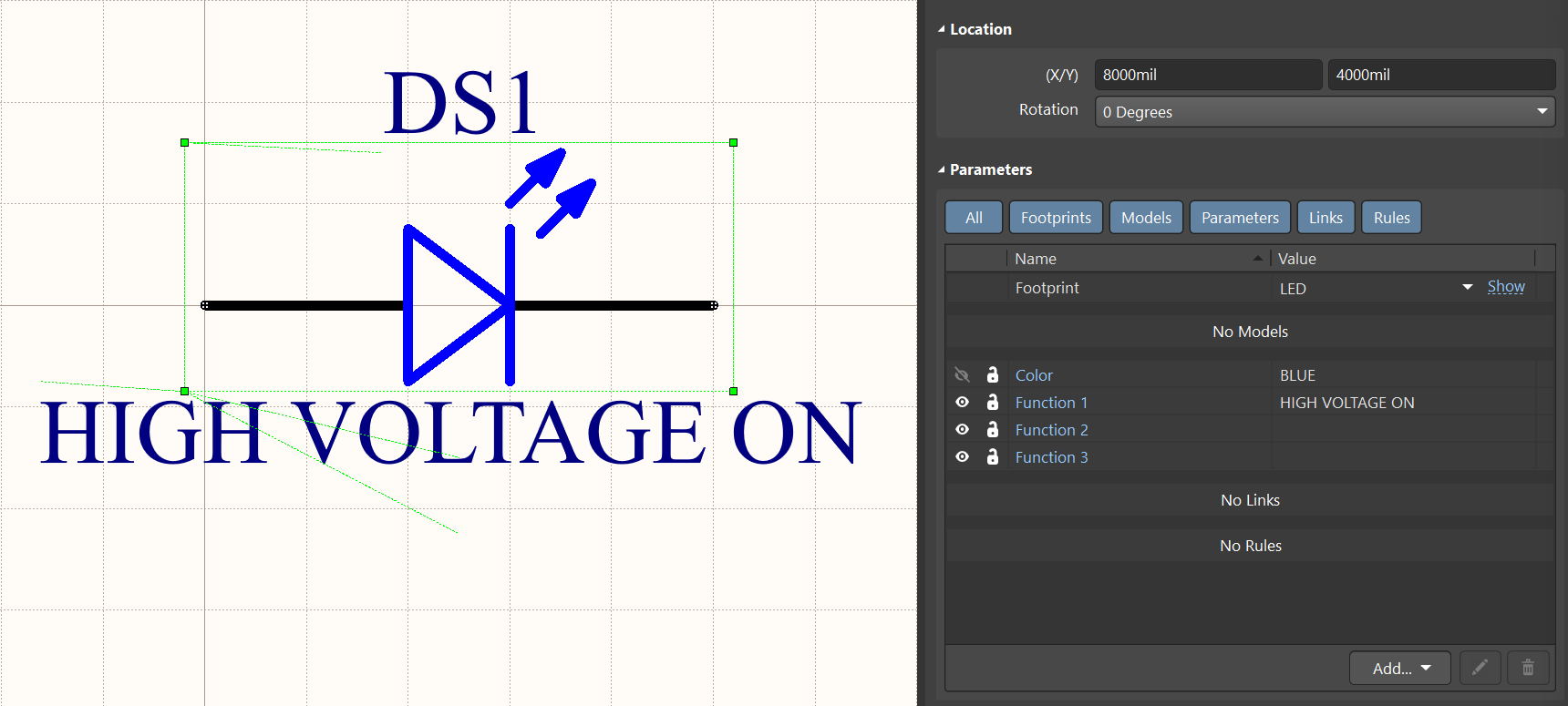
PCB:
In this last example, all three label parameters are used to label the LED on the board similar to the previous example so the label can fit better on the board under a higher density condition. This illustrates why it is important to have at least three label parameters in the component.
Schematic:
PCB: