




대체 부품


Price @ 1000
$ 0.533
$ 25.65
$ 25.65
Stock
388,278
225,490
225,490
Authorized Distributors
5
1
1
Case/Package
SSOP
SSOP
SSOP
Number of Pins
20
20
20
Logic Function
D-Type, Flip-Flop
D-Type, Flip-Flop
D-Type, Flip-Flop
Number of Elements
1
1
1
Number of Bits per Element
8
8
8
Propagation Delay
6.6 ns
5 ns
5 ns
Frequency
200 MHz
150 MHz
150 MHz
Clock Edge Trigger Type
Positive Edge
Positive Edge
Positive Edge
Min Supply Voltage
4.5 V
4.5 V
4.5 V
Max Supply Voltage
5.5 V
5.5 V
5.5 V
Quiescent Current
30 mA
-
-
공급망
Lifecycle StatusProduction (Last Updated: 1 week ago)
Manufacturer Lifecycle StatusACTIVE (Last Updated: 1 week ago)
엔지니어링 리소스
Texas Instruments SN74ABT574ADBR의 평가 키트와 참조 설계를 확인하세요.
평가 키트
관련 부품
Texas InstrumentsSN74ABT273DBR
Flip Flop D-Type Bus Interface Pos-Edge 1-Element 20-Pin SSOP T/R

Texas InstrumentsSN74ABT374ADBR
Octal Edge-Triggered D-Type Flip-Flops with 3-State Outputs 20-SSOP -40 to 85

NXP Semiconductors74ABT273ADB,118
D Flip-Flop, ABT Series, 1-Func, Positive Edge Triggered, 8-Bit, True Output, BICMOS, PDSO20

onsemi74ABT273CMSA
D Flip-Flop, ABT Series, 1-Func, Positive Edge Triggered, 8-Bit, True Output, BICMOS, PDSO20


설명
유통업체에서 제공한 Texas Instruments SN74ABT574ADBR에 대한 설명입니다.
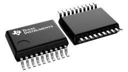
Flip Flop D-Type Bus Interface Pos-Edge 3-ST 1-Element 20-Pin SSOP T/R
Cut Tape (CT) 74ABT574 e4 74ABT flip flop 7.2mm 6.6ns @ 5V 50pF 200MHz 6.6ns
Positive edge 250μA 6.6ns@ 5V,50pF Non-inverting Tristate,Non-inverting 1 4.5V 5.5V 64mA Standard ABT TTL 3.5pF 32mA 200MHz SSOP-20 SMD mount,glue mount 7.2mm*5.3mm*1.95mm
Flip-Flop Logic IC; Logic Family:ABT; Supply Voltage Min:4.5V; Supply Voltage Max:5.5V; Package/Case:20-SSOP; No. of Pins:20; Operating Temperature Range:-40°C to +85°C; Input Type:TTL; Leaded Process Compatible:Yes ;RoHS Compliant: Yes
These 8-bit flip-flops feature 3-state outputs designed specifically for driving highly capacitive or relatively low-impedance loads. They are particularly suitable for implementing buffer registers, I/O ports, bidirectional bus drivers, and working registers. The eight flip-flops of the SN54ABT574 and SN74ABT574A are edge-triggered D-type flip-flops. On the positive transition of the clock (CLK) input, the Q outputs are set to the logic levels set up at the data (D) inputs. A buffered output-enable (OE)\ input can be used to place the eight outputs in either a normal logic state (high or low logic levels) or the high-impedance state. In the high-impedance state, the outputs neither load nor drive the bus lines significantly. The high-impedance state and increased drive provide the capability to drive bus lines without need for interface or pullup components. OE\ does not affect the internal operations of the flip-flops. Old data can be retained or new data can be entered while the outputs are in the high-impedance state. To ensure the high-impedance state during power up or power down, OE\ should be tied to VCC through a pullup resistor; the minimum value of the resistor is determined by the current-sinking capability of the driver. This device is fully specified for partial-power-down applications using Ioff. The Ioff circuitry disables the outputs, preventing damaging current backflow through the device when it is powered down.
제조업체 별칭
Texas Instruments에는 유통업체가 대체하여 사용할 수 있는 전 세계 여러 브랜드가 있습니다. Texas Instruments는 다음 이름으로도 알려져 있습니다:
- TI
- TEXAS
- TEXAS INST
- TEXAS INSTR
- TEXAS INSTRUMENT
- TEXAS INSTRUMENTS INC
- TEXAS INS
- TEXAS INSTRU
- TEXAS INSTRUMEN
- TI/NS
- TEX
- Texas Instruments (TI)
- TEXASIN
- TEXAS INSTRUMENTS INCORPORATED
- TEXINS
- TEXAS INTRUMENTS
- TEAXS
- TEXASI
- TI Texas Instruments
- TEXAS INSTRUM
- TEXAS USD
- TEXAS INSRUMENTS
- TEXAS INSRUMENT
- TEXAS INSTUMENTS
- TI-ROHS
- Texas Instr.
- Texas Instruments Inc.
기술 사양
Physical
Case/PackageSSOP
Contact PlatingGold
MountSurface Mount
Number of Pins20
Weight156.687814 mg
Technical
Clock Edge Trigger TypePositive Edge
Frequency200 MHz
High Level Output Current-32 mA
Logic FunctionD-Type, Flip-Flop
Low Level Output Current64 mA
Max Operating Temperature85 °C
Max Supply Voltage5.5 V
Min Operating Temperature-40 °C
Min Supply Voltage4.5 V
Number of Bits8
Number of Bits per Element8
Number of Channels8
Number of Circuits8
Number of Elements1
Number of Input Lines8
Number of Output Lines3
Number of Outputs8
Operating Supply Voltage5 V
Output Current64 mA
Output TypeTTL
PackagingTape & Reel
PolarityNon-Inverting
Propagation Delay6.6 ns
Quiescent Current30 mA
Schedule B8542390000
Turn-On Delay Time3.9 ns
Dimensions
Height2 mm
Length7.2 mm
Thickness1.95 mm
Width5.3 mm