



CADモデル
製造元 onsemi FDFMA3N109 のシンボル、フットプリント、3D STEPモデルを信頼できるパートナーからダウンロードする
| ソース | eCAD | mCAD | ファイル |
|---|---|---|---|
 SnapEDA | フットプリント | ダウンロード |
CADモデルをダウンロードする際に、パートナーサイトが新しいタブで開きます。
OctopartからCADモデルをダウンロードすることにより、お客様は弊社の利用規約とプライバシーポリシーに同意したものとみなされます。
サプライチェーン
Country of OriginThailand
Export Control Classification Number (ECCN) CodeEAR99
Harmonized Tariff Schedule (HTS) Code8541.29.00.95
Introduction Date2006-05-26
Lifecycle StatusObsolete (Last Updated: 2 weeks ago)
LTB Date2021-10-08
LTD Date2022-04-08
Manufacturer Lifecycle StatusOBSOLETE (Last Updated: 2 weeks ago)
関連部品


VishaySI1443EDH-T1-GE3
MOSFET, P-CH, -30V, -4A, SOT-363-6; Transistor Polarity:P Channel; Continuous Dr


VishaySI1539CDL-T1-GE3
Dual MOSFET, Complementary N and P Channel, 30 V, 30 V, 700 mA, 700 mA, 0.323 ohm

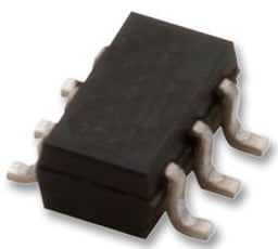
説明
onsemi FDFMA3N109の詳細は販売業者から提供されます。
Integrated N-Channel PowerTrench®MOSFET and Schottky Diode 30 V, 2.9 A, 123 mΩ
30V,2.9A ,INTEGRATED, NCH POWER MOSFET & SCHOTTKY DIODE
Trans MOSFET N-CH 30V 2.9A 6-Pin MicroFET EP T/R
Small Signal Field-Effect Transistor, 2.9A I(D), 30V, 1-Element, N-Channel, Silicon, Metal-oxide Semiconductor FET
MOSFET N-CH 30V 2.9A 6MICROFET
SMALL SIGNAL FIELD-EFFECT TRANSI
MOSFET, N, MLP6; Transistor Polarity:N Channel; Continuous Drain Current Id:2.9A; Drain Source Voltage Vds:30V; On Resistance Rds(on):123mohm; Rds(on) Test Voltage Vgs:1V; Threshold Voltage Vgs Typ:1V; Power Dissipation Pd:1.5W; Operating Temperature Range:-55°C to +150°C; Transistor Case Style:MicroFET; No. of Pins:8; SVHC:No SVHC (20-Jun-2011); Current Id Max:2.9A; Current Temperature:25°C; Full Power Rating Temperature:25°C; Junction Temperature Tj Max:150°C; Junction Temperature Tj Min:-55°C; Package / Case:MLP-6; Power Dissipation Pd:1.5W; Power Dissipation Pd:1.5W; Pulse Current Idm:10A; SMD Marking:109; Termination Type:SMD; Voltage Vds:30V; Voltage Vds Typ:30V; Voltage Vgs Max:12V; Voltage Vgs Rds on Measurement:4.5V
This device is designed specifically as a single package solution for a boost topology in cellular handset and other ultra-portable applications. It features a MOSFET with low input capacitance, total gate charge and onstate resistance, and an independently connected schottky diode with low forward voltage and reverse leakage current to maximize boost efficiency. The MicroFET 2x2 package offers exceptional thermal performance for its physical size and is well suited to switching and linear mode applications.
メーカーの別名
onsemiは世界中でいくつかのブランドを持っており、販売業者が代替名として使用するかもしれません。 onsemi は以下の名前でも知られているかもしれません:
- ON Semiconductor
- ONS
- ONSEMICON
- ON SEM
- ON SEMICONDUCTO
- ON SEMICONDUCTORS
- ONSEMIC
- ON Semicondu
- OSC
- ONSE
- ON Semiconductor / Fairchild
- ON SEMICOND
- SCG
- ON Semiconductor Cor
- ON SEMICO
- ONSM
- onsemi / Fairchild
- ON SEMICONDUCTOR CORP
- MOT/ON SEMI
- Fairchild/ONSemiconductor
- ON Semiconductor Corporation
- ON4
- ON Semi - ON Semiconductor
- ON SEMICONDUCT
- ON-SEMI SCG
- ON Semiconductor Inc.
- onsemiconductor
- On Semiconductor Ltd
技術仕様
Physical
Case/PackageSOT-363
MountSurface Mount
Number of Pins6
Number of Terminals6
Weight60 mg
Technical
Continuous Drain Current (ID)2.9 A
Current Rating2.9 A
Drain to Source Breakdown Voltage30 V
Drain to Source Resistance123 mΩ
Drain to Source Voltage (Vds)30 V
Element ConfigurationSingle
Fall Time8 ns
Gate to Source Voltage (Vgs)12 V
Input Capacitance220 pF
Max Operating Temperature150 °C
Max Power Dissipation1.5 W
Min Breakdown Voltage30 V
Min Operating Temperature-55 °C
Number of Elements1
PackagingCut Tape
Power Dissipation1.5 W
Rds On Max123 mΩ
Resistance123 MΩ
Rise Time8 ns
Schedule B8541290080
Threshold Voltage1 V
Turn-Off Delay Time12 ns
Turn-On Delay Time6 ns
Voltage Rating (DC)30 V
Dimensions
Height750 µm
Length2 mm
Width2 mm
コンプライアンス
環境分類
China RoHSCompliant
Lead FreeLead Free
Radiation HardeningNo
REACH SVHCUnaffected
RoHSCompliant
準拠ステートメント