Previous article
How to Drive a Servo Motor and the Components You Need
Octopart Staff
Field effect transistors (FETs) are today’s workhorses for digital logic, but they enjoy plenty of applications outside of digital integrated circuits, everything from motor drivers to voltage regulators and specialty amplifiers can make use of different types of FETs, and there are some useful advantages that make discrete FETs more desirable compared to their bipolar junction transistor (BJT) cousins.
Although advanced components and applications are continually focusing on fundamentally modifying and optimizing FET architecture, discrete BJTs and FETs are here to stay. Each of the various types of FETs has its place in different systems, and designers can find the exact FETs they need with the best set of supply chain tools. If you’re unsure which type of FET you should use, read our guide to learn more about different FETs and which specifications are most important.
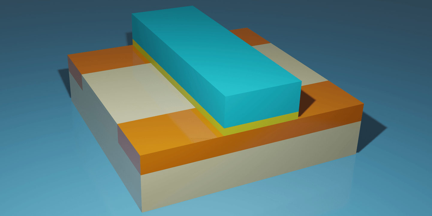
Field effect transistors, or simply FETs, form the basis of modern digital integrated circuits. Just like earlier BJTs, FETs are three-terminal switches (four if you include the body terminal in a MOSFET), where a voltage is applied to the gate to control the current flowing between the source and drain. Once the voltage is applied to the gate region, the channel resistance switches states as a function of the input voltage. These are the very basics of different types of FETs.
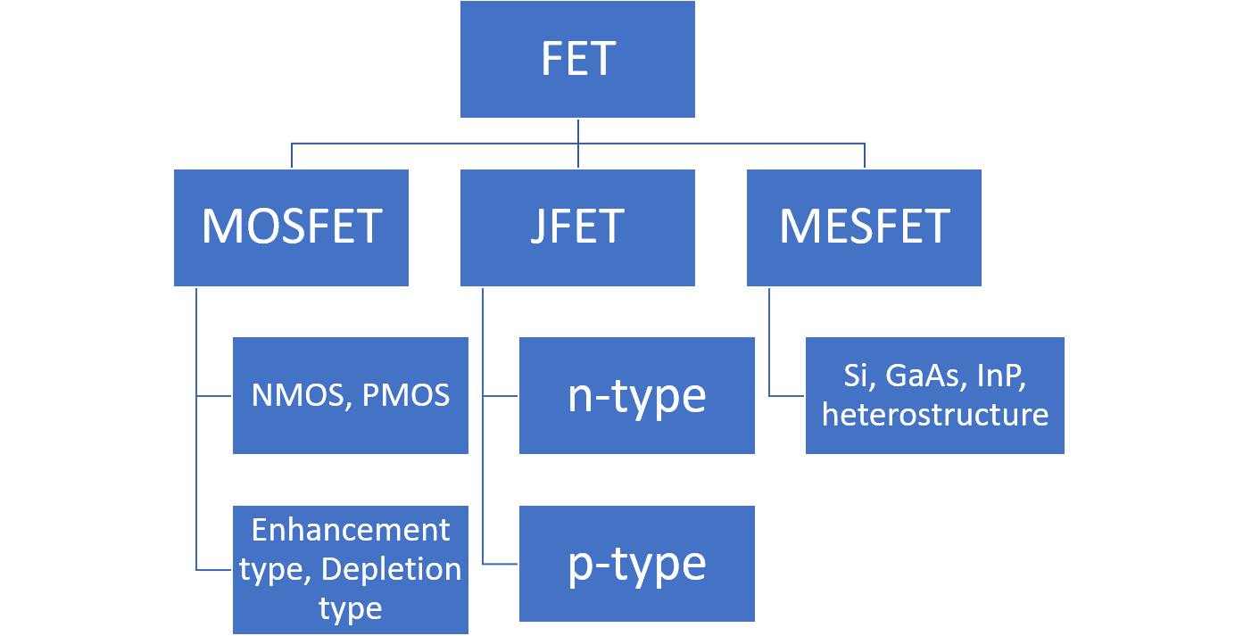
FETs are subdivided into three different types: insulated gate FETs (better known as MOSFETs), junction FETs (JFETs), and metal-semiconductor FET (MESFET). The flowchart below briefly summarizes these three types of FETs and their sub-types. Among the different types of MOSFETs, the choice of enhancement type or depletion type FETs gives designers some flexibility as to how they implement switching in their systems (e.g., in power regulators).
With so many different types of FETs to choose from, which is best and how do they stack up to BJTs? Let’s dig a little deeper to see which types of FETs matter for different applications.
MESFETs are often used as drivers or switches in RF applications requiring high power output. Commercial MESFET components are available in a range of packages; SO/SOIC/SOP packaged components are available with bandwidth reaching ~8 GHz, while high frequencies reaching ~30 GHz can be accessed in QFN packages. High frequency MESFETs are normally made from SiGe (low moderate power output) or GaAs (for high power output), and you’ll find these structures integrated into high frequency SoCs.
Among the various types of FETs, MOSFETs probably enjoy the broadest range of practical applications. These components find their place in many power electronics applications as they can handle switching powers reaching kW levels. And of course, anyone who is familiar with modern CMOS logic circuits should know that MOSFETs form the basis for CMOS devices.
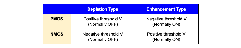
If you need to pick a discrete MOSFET for a switching application, then how the device is switched is quite important as you’ll need to select the correct voltage polarity applied to the gate region. Enhancement type NMOS is often used as a switching element in applications like power regulation and conditioning at high voltage/current; I find it makes grounding and layout easier as you only need to source positive voltages around a board.
JFETs also come in the n and p channel varieties, where n-channel is normally used as electrons have greater mobility than holes. JFETs also have a breakdown region when the drain-source voltage is sufficiently high (analogous to pn diode breakdown). Compared to MOSFETs, JEFTs have the following characteristics:
Depletion mode only
Lower frequency drift
Lower input impedance
High drain resistance gives flatter transfer curves
Higher input capacitance
Their lower frequency drift makes them more desirable in oscillators or precision timing circuits. The higher input capacitance leads to slightly longer turn-on times when used as switches. Although they might be useful for oscillators, when used in amplifiers they tend to have a relatively low gain-bandwidth product compared to MOSFETs and much lower than comparable MESFETs.
High electron mobility transistors (HEMTs) refers to something closer to materials used in FETs, rather than a totally different structure or type of circuit. HEMTs may be used in RF devices that must source power at high frequencies, or that switch at fast edge rates. The typical materials used in these devices are GaAs and GaN, both of which are used in commercially available components. These devices are designed to provide high power output at frequencies reaching into the mmWave range. Other III-V materials like InP have been researched for use in HEMTs. However, these materials are not yet producible in standard component processes at scale.
Because HEMT applications overlap with MESFETs, it’s fair to ask what the difference is between these materials. The difference appears in the transistor’s epitaxial layer. HEMTs are heterostructure devices that use compositionally different stacked layers of material with higher electron mobility than the bulk material in the device. In GaAs HEMTs, the common material used in the epitaxial layer is nonstoichiometric AlGaAs. We do not see these same structures or materials in MESFETs.
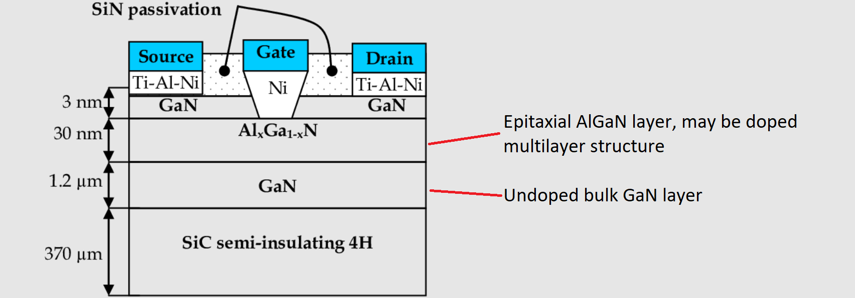
A similar approach with a nonstoichiometric layer is used in GaN HEMTs, where the epitaxial layer is AlGaN. An example HEMT structure on a SiC substrate is shown below. In this structure, the AlGaN layer may be a doped multilayer structure, and the conduction channel will be formed in this portion of the device.
The high mobility of electrons in the conducting channel provides much more efficient power delivery at high GHz frequencies. These systems provide higher power handling, higher frequencies, and greater heat dissipation (particularly with SiC) compared to scaled Si MOSFETs operating in mmWave bands. For these reasons, GaN HEMTs have also seen usage in power electronics as a highly thermally conductive replacement for Si MOSFETs.
Much as we’d like to list every specification found on a data sheet, not all specifications are relevant for every application. There are a few that are universal for almost any application:
On-state resistance: This is one of the most important specifications as it determines the efficiency of a FET in power delivery and switching.
Leakage current: Even in the off-state, there is some minor amount of current that flows between the source and drain, leading to some power loss in the OFF state.
Terminal capacitances: These values for capacitances will limit switching time in the device. This is not normally important unless you are designing a high frequency analog product.
Absolute maximum temperature: FETs will fail if the channel temperature reaches its maximum rated value. There is normally a small factor of safety here, but these components need to be selected while considering the environment where they’ll be deployed.
Voltage/current rating: This pair of values is specified for a particular driving method (DC, pulsed, or harmonic) and will determine the safe operating area of a FET. Once these specifications are exceeded for a particular FET, the device could experience breakdown and will fail.
The last point is important as it relates to the safe operating area of a FET. All FETs have a combination of source-to-drain voltage (V(DS)) and drain current (I(D)) within which a FET can be operated without failing. This combination of voltages, currents, and driving methods forms the safe operating area for a MOSFET, which can be traced out on a graph.
An example of the safe operating area of a MOSFET (FDD7N25LZTM from ON Semiconductor) is shown below. In this graph, DC driving is being compared with AC driving at different conditions (in this case, pulsed driving). For DC driving, the safe operating area boundary will be closer to the origin compared to driving with shorter pulses. The reason the safe operating area expands when the pulse duration is shorter is because the average current will be lower, assuming the same pulse repetition frequency.
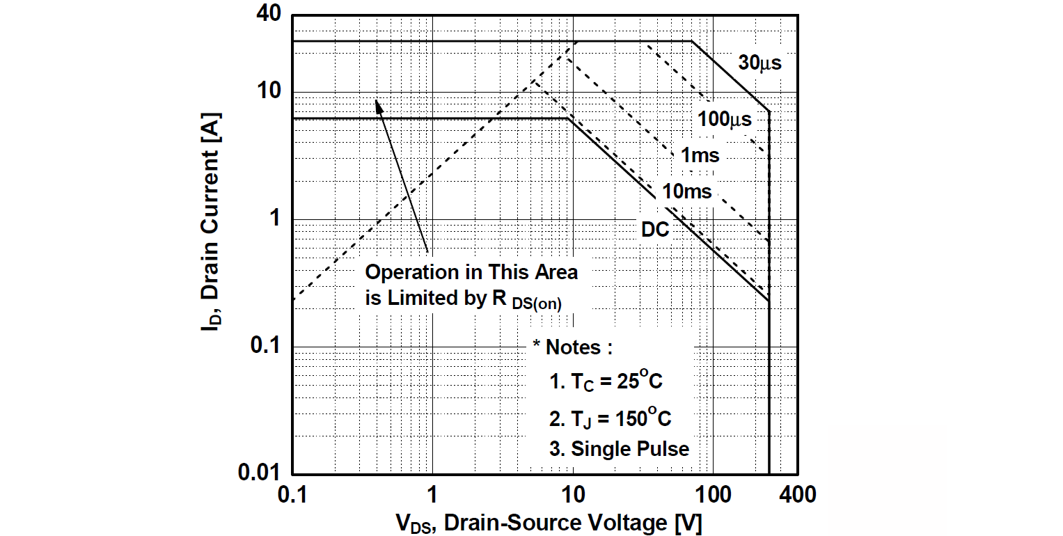
In total, there are three primary factors that determine the safe operating area of a FET:
Steady-state temperature of the junction
ON-state resistance
Driving method (DC, AC, etc.)
In general, any AC driving that matches the average current of a DC driver will have a similar safe operating area. When the average current in AC driving decreases, the safe operating area will expand. This can be used as a simple metric to select a MOSFET for use in power delivery applications: simply compare the average current under AC driving with the DC driving current under similar operating parameters (V(DS) and I(D)) to determine whether the MOSFET will be reliable under AC driving.
The other factor that is more difficult to address is the temperature of the MOSFET, specifically the junction temperature. If the junction temperature is too large, then the MOSFET is at risk of failing. For an accurate comparison with the safe operating area, it is necessary to determine the power loss in the ON state and use the thermal resistance of the component to predict the equilibrium temperature. In general, higher junction temperature leads to smaller safe operating areas.
No matter which types of FETs you need for your new product, you can use the advanced search and filtration features in Octopart to find the parts you need. When you use Octopart’s electronics search engine, you’ll have access to distributor data and parts specifications, all of which are freely accessible in a user-friendly interface. Take a look at our linear integrated circuits page to find the components you need.
Stay up-to-date with our latest articles by signing up for our newsletter.