Previous article
IoT and Mobile SoCs: Processing Power for Next-gen Devices
Octopart Staff
Power supplies and power management systems play a critical role in extending a mobile device’s battery life and performance. As a critical part of these systems, a voltage regulator is designed to maintain the output voltage from a power supply at a constant value. There are a number of points to consider when choosing a voltage regulator for a mobile or IoT device. While this often involves a tradeoff between noise, thermal management, and deviations from regulation, finding the right balance between these points can help ensure that your next mobile device operates as desired.
Any voltage regulator needs to provide some specific functions. First, the regulator needs to step up or down the voltage between the battery and different sub-circuits in the device. Step-up functionality is required by high-voltage devices like OLEDs, while the step down function helps reduce the power consumed by digital CMOS circuits. This provides longer battery life and enables new features like additional cameras and haptic feedback without a significant impact on battery size.
Noise management and power isolation are critical in mobile devices in order to ensure signal integrity. State of the art RF modulation schemes for Gbps data rates place stringent requirements on distortion and interference artifacts. These mandate that careful attention be paid to all noise sources, especially conducted and radiated EMI from the power supply.
In terms of power isolation, a good voltage regulator should also prevent changes in the battery’s output voltage from propagating transient signals through the output (such as those introduced by a pulsed RF power amplifier), thereby affecting downstream circuits. Finally, any voltage regulator for any mobile device, whether it is a smartphone, wearable device, IoT, or other device, must have a small footprint and low cost while still extending battery life.
Linear regulators: These are typically made up of a reference voltage generator, error amplifier, power transistor, resistive divider to monitor the output voltage, and decoupling capacitor to ensure the voltage on a power bus is stable. Low-dropout (LDO) regulators based on pnp and pFET transistors exhibit different quiescent current characteristics during dropout, depending on the transistor polarity. pFET transistors draw virtually no current and exhibit no quiescent rise during dropout, while nFETs exhibit a rise in quiescent current as the input voltage rises and nears the output voltage.
The advantages or linear converters are their low noise and ripple, small to medium size, and their low complexity and cost. The disadvantages include step-down operation only, and they have low to medium efficiency, although this depends on the load current, battery voltage, and heat dissipation.
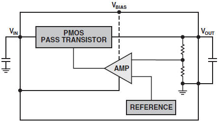 A linear regulator. Figure in The Fundamentals of LDO Design and Applications. Available from Analog Devices
Switched capacitor regulators: Also referred to as charge-pump converters, these use capacitors and several switches to provide an output voltage higher or lower than the input voltage. They store and transfer energy from the input to output in a flying capacitor connected to digital switches.
The advantages of charge-pump converters include high efficiency and low radiated EMI compared to other voltage regulators. This is due to the use of a capacitor for storage energy and transfer, which enables the use of soft switching techniques to control the digital switches. These converters do not use feedback to achieve regulation, relying instead on the switching period duty cycle to compensate for changes in the output voltage. These controllers are usually restricted to low-power applications.
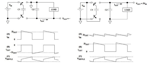 Switched capacitor regulator circuit diagrams and input/output waveforms
Switching regulators: These regulators can step the input voltage up (boost) or down (buck); they are also capable of inverting its polarity. The typical buck-boost converter consists of a switch network that generates an AC signal, a low-pass filter that passes the DC component of this signal to the output, and a feedback network to regulate the output voltage by changing the AC signal’s duty cycle or frequency.
A switching regulator’s output voltage characteristics depend largely on the quality of the low pass filter, which is implemented as an LC circuit. The output voltage ripple noise and regulator efficiency are largely dependent on the size of the inductor, where larger inductors reduce the ripple and the circuit efficiency due to their larger energy losses through their equivalent series resistance. These regulator circuits waste less heat, but they are generally more complex, bigger, and costlier than their linear counterparts.
Combining linear and switch-mode regulators is a common technique for generating multiple supply voltages in a mobile device. The power supply designer needs to consider the characteristics of the power source (battery) and load to choose the optimal circuit solution for a particular sub-circuit. For example, as mobile device processors are fabricated using progressively finer transistor architecture (10 nm or less), which reduces their supply voltage and current requirements, the quiescent current of the regulator circuit becomes a larger percentage of the load current and has a greater impact on the circuit efficiency.
The MAX8863 linear voltage regulator provides higher reliable supply voltage (2.5 V to 6.5 V) with up to 120 mA output current in a miniature 5-pin SOT23 package. The device uses a PMOS pass transistor, allowing the 80 µA supply current to remain independent of load. These devices are ideal for battery-operated portable equipment such as cellular phones or other IoT devices which operate with a variety of signalling standards. An external resistor divider network can also be used to adjust the output voltage:
The devices feature Dual Mode™ operation: their output voltage is preset...or can be adjusted with an external resistor divider. Other features include low-power shutdown, short-circuit protection, thermal shutdown protection, and reverse battery protection. [From the MAX8863 datasheet]
The MAX8864, a variant of the MAX8863, also includes an auto-discharge function. This feature actively discharges the output voltage to ground when the device is placed in shutdown mode.
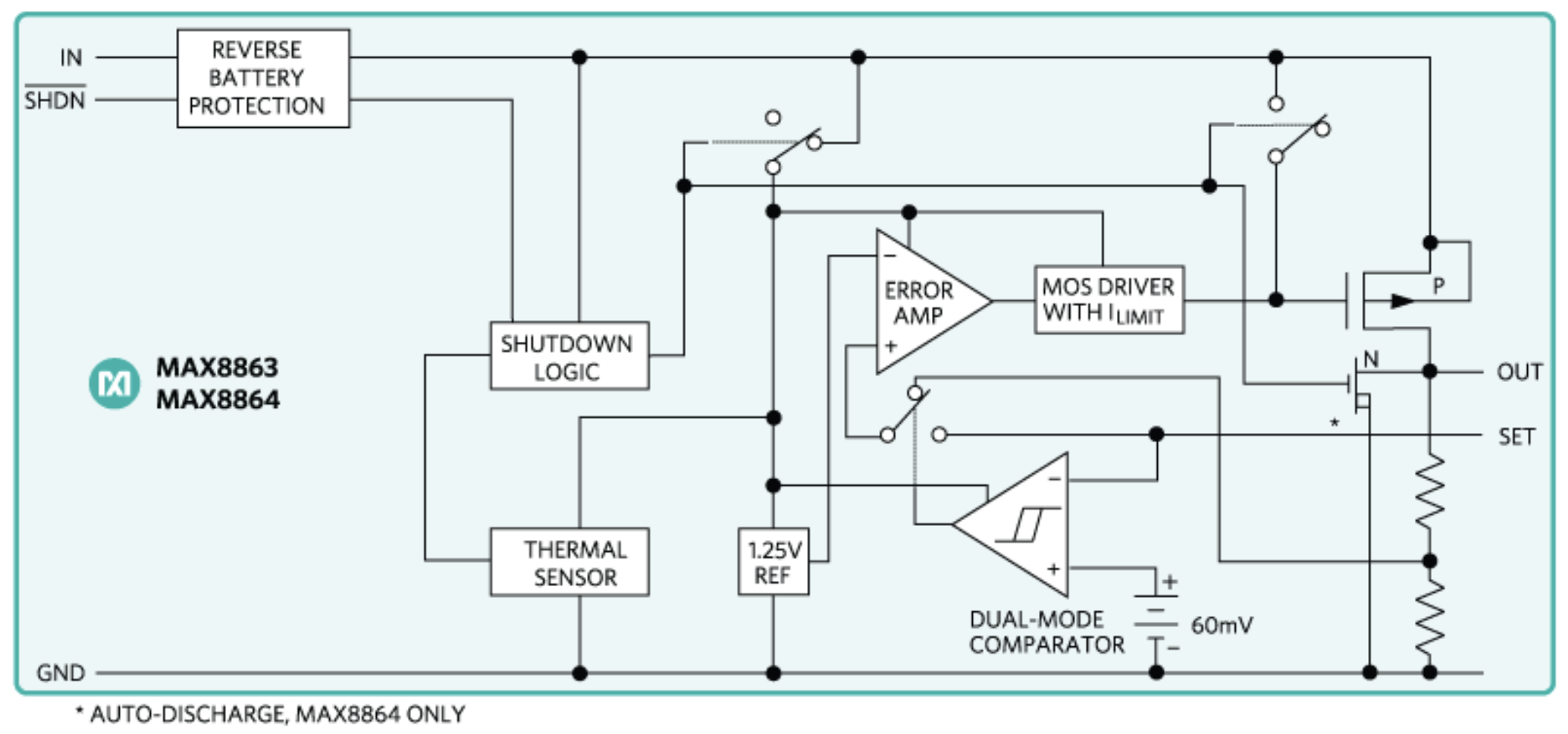 Functional block diagram, from Maxim Integrated
Everyone loves taking selfies, and plenty of folks need to teleconference via their laptops. These activities, and devices that make copious use of LEDs, require a voltage regulator that can provide stable output for these particular components. The MAX1576 switched capacitor regulator is designed to regulate backlighting and camera flash with up to 8 white LEDs in mobile devices (24-pin thin QFN, 4 mm x 4 mm package). Four LEDs can be driven at up to 30 mA for backlighting, while the remaining four LEDs in the flash group can be pulsed up to 100 mA per LED:
The MAX1576 uses two external resistors to set the main and flash full-scale (100%) LED currents. Four control pins are used for LED dimming by either serial control or 2-bit logic per group. ENM1 and ENM2 set the main LEDs to 10%, 30%, or 100% of full scale. ENF1 and ENF2 set the flash LEDs to 20%, 40%, or 100% of full scale. In addition, connect either pair of control pins together for single-wire, serial pulse dimming control.
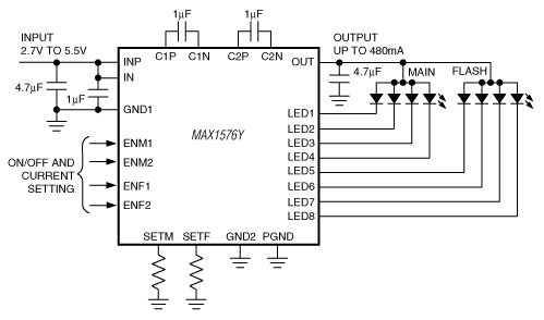 Pin diagram and example circuit with the MAX1576 switch capacitor regulator (from the MAX1576 datasheet)
The LT1738 switching regulator from Analog Devices is a slew rate controlled DC/DC controller with ultra low noise. Switching regulators are known to be quite noisy due to the PWM switching signal, but the LT1738 uses a controlled voltage and current slew rates in an external N-channel MOSFET switch. This device emits much less intense radiated noise than other switching regulators with similar power output and footprint, making it an excellent choice for use in new mobile and IoT devices.
Current and voltage slew rates can be independently set to optimize harmonic content of the switching waveforms vs efficiency. The LT1738 can reduce high frequency harmonic power by as much as 40 dB with only minor losses in efficiency. The LT1738 utilizes a current mode architecture optimized for single switch topologies...The internal oscillator may be synchronized to an external clock for more accurate placement of switching harmonics.
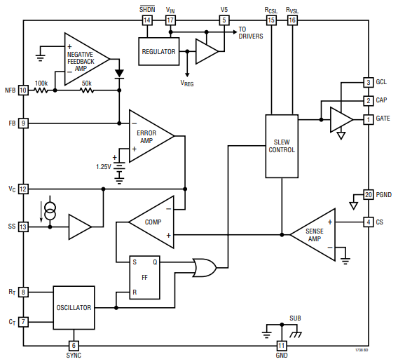 Block diagram of the LT1738 switching regulator (from the LT1738 datasheet).
Your next mobile or IoT device needs to conserve and properly manage power in order to extend its usable lifetime. You can make this happen with the right voltage regulator and other components specifically designed for mobile and IoT applications. Try using our Part Selector guide to determine the best option for your next product.
Don't miss out on articles like this one! Stay up-to-date with our latest articles by signing up for our newsletter!